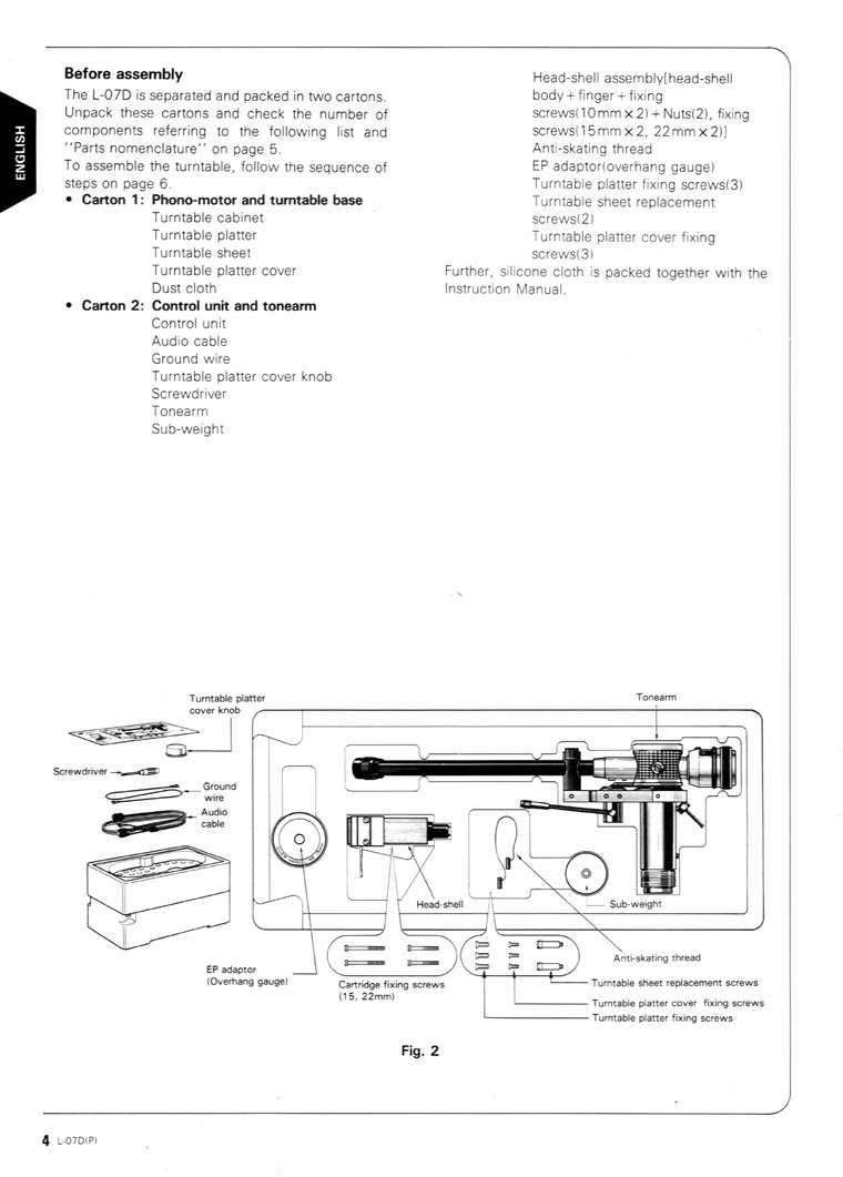
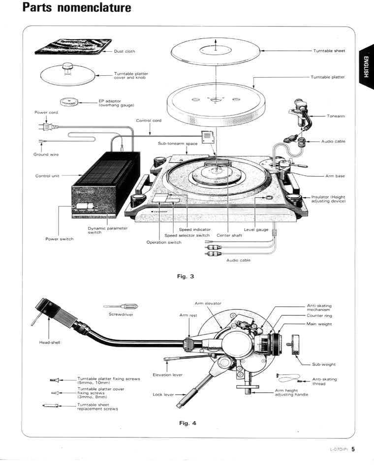
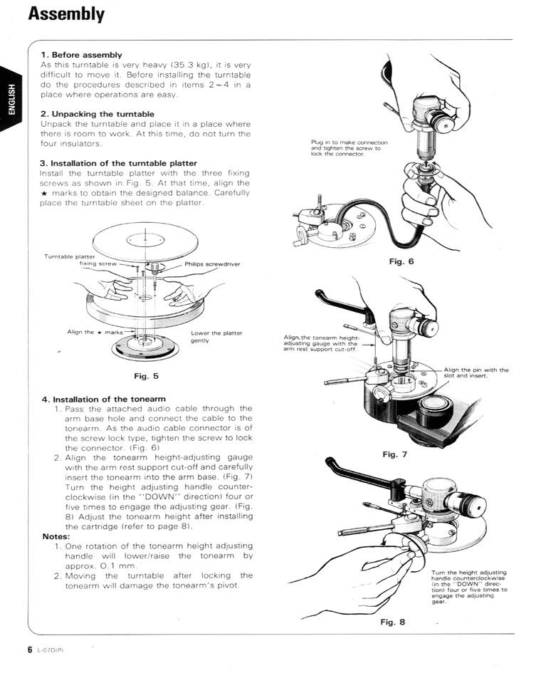
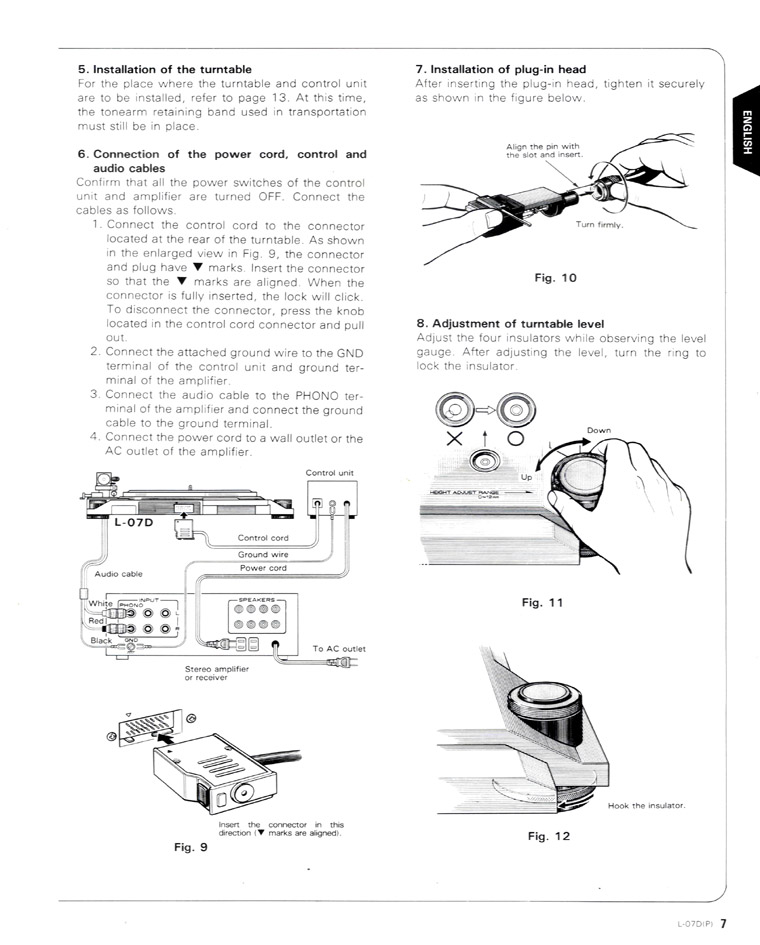
![]()
![]()
![]()
![]()
![]()
![]()
![]()
![]()
![]()
![]()
![]()
![]()
![]()
![]()
![]()
![]()
![]()
![]()
![]()
![]()
![]()
![]()
![]()
![]()
![]()
![]()
![]()
![]()
![]()
![]()
Literature
Literature pertinent to the L-07D includes the instruction manuals, the service manuals, the sales brochure, the DS-20 Outer Disc Stabilizer Guide Book and the TS-10 Turntable Sheet Guide Book. All of the above referenced literature booklets are available on this page for viewing and printing. I have set the page size, such that each page should print out on a single sheet of paper on a standard printer.
I have also created some documents which I have developed from the L-07D & L-07D II schematics and service manuals. These documents help me troubleshoot and repair these decks. On this page, the above referenced documents are available for display below.
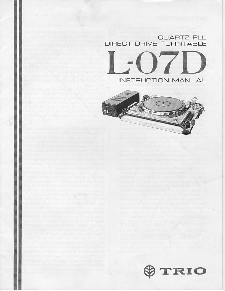
L-07D Instruction Manual in English
The pages below are from the North American L-07D instruction manual:
L-07D Instruction Manual in English in PDF format
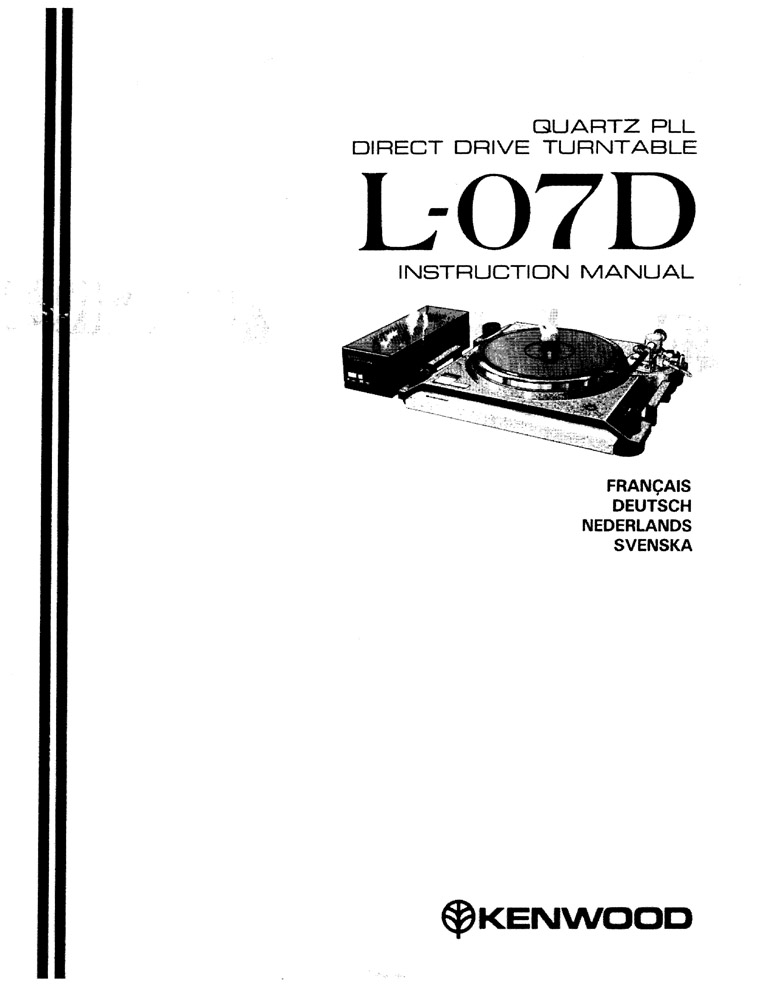
L-07D Instruction Manual in French - German - Dutch - Swedish
The pages below are from the French/German/Netherlands/Swedish L-07D instruction manual:
L-07D Instruction Manual in French - German - Dutch - Swedish in PDF format
L-07D II Instruction Manual in English - French - Spanish
The pages below are from the English/French/Spanish L-07D II instruction manual:
L-07D II Instruction Manual in English - French - Spanish in PDF format
L-07D Service Manual in English
L-07D Service Manual in English in PDF format
L-07D Service Manual in English in PDF format (300 dpi color scan)
Switching PC Board and LED PC Board
Schematic Four Pages (600 dpi)
L-07D II Service Manual in English
L-07D II Service Manual in English in PDF format
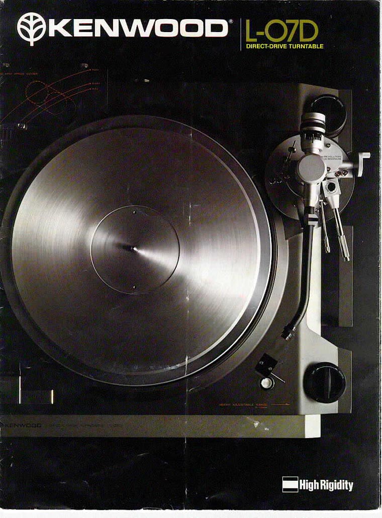
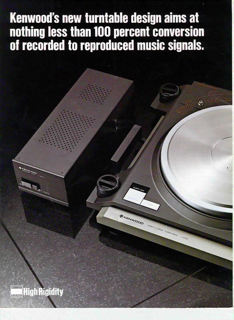
L-07D Brochure
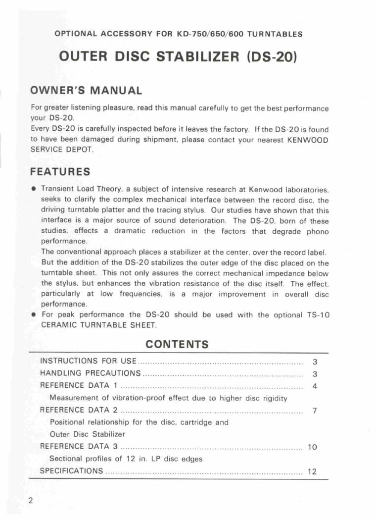
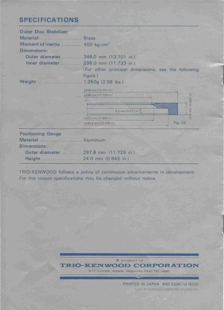
DS-20 Outer Disc Stabilizer Guide Book
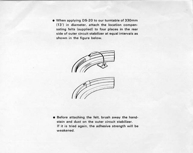
Compensating Felt Application Instructions
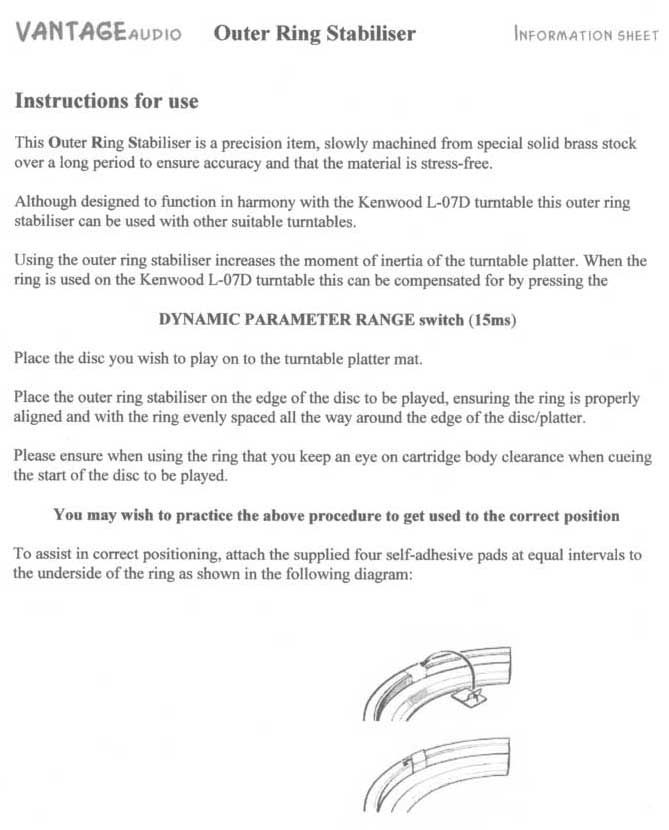
DS-20 Outer Ring Stabiliser Reproduction Information Sheet
Information Sheet from Vantage Audio
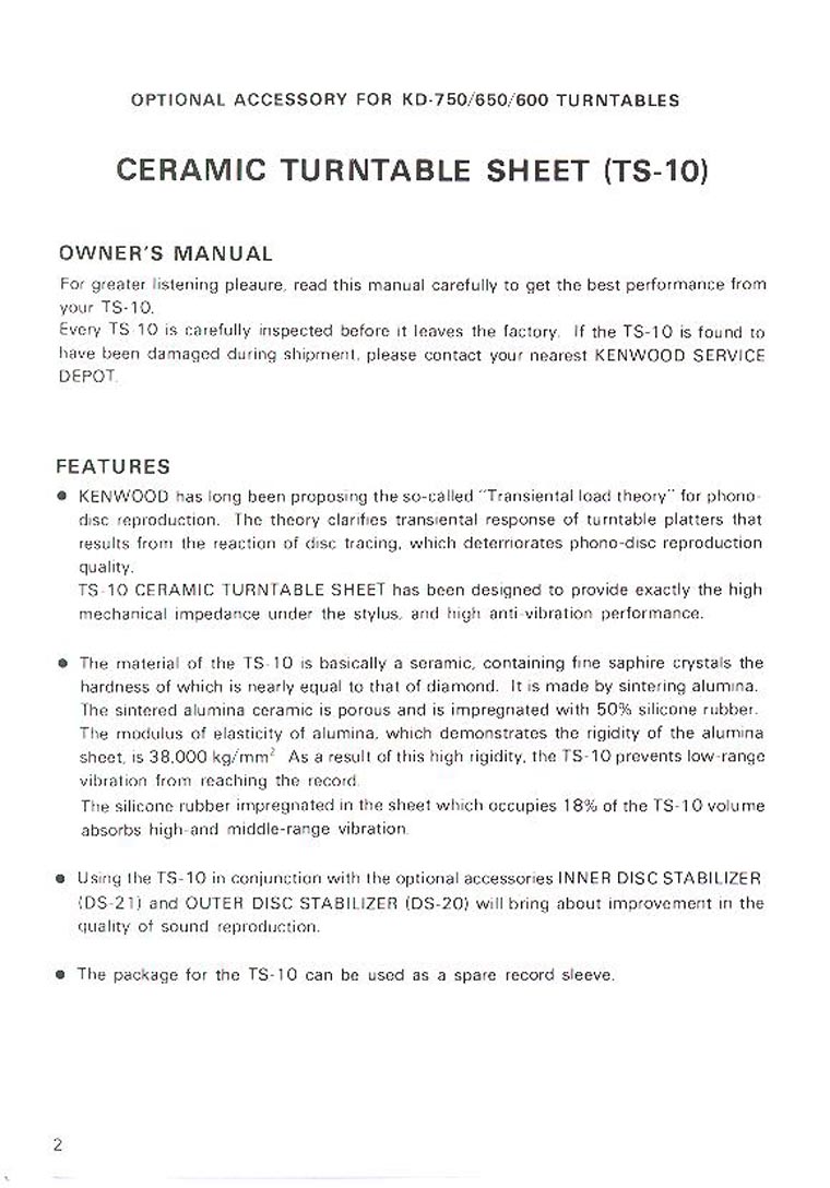
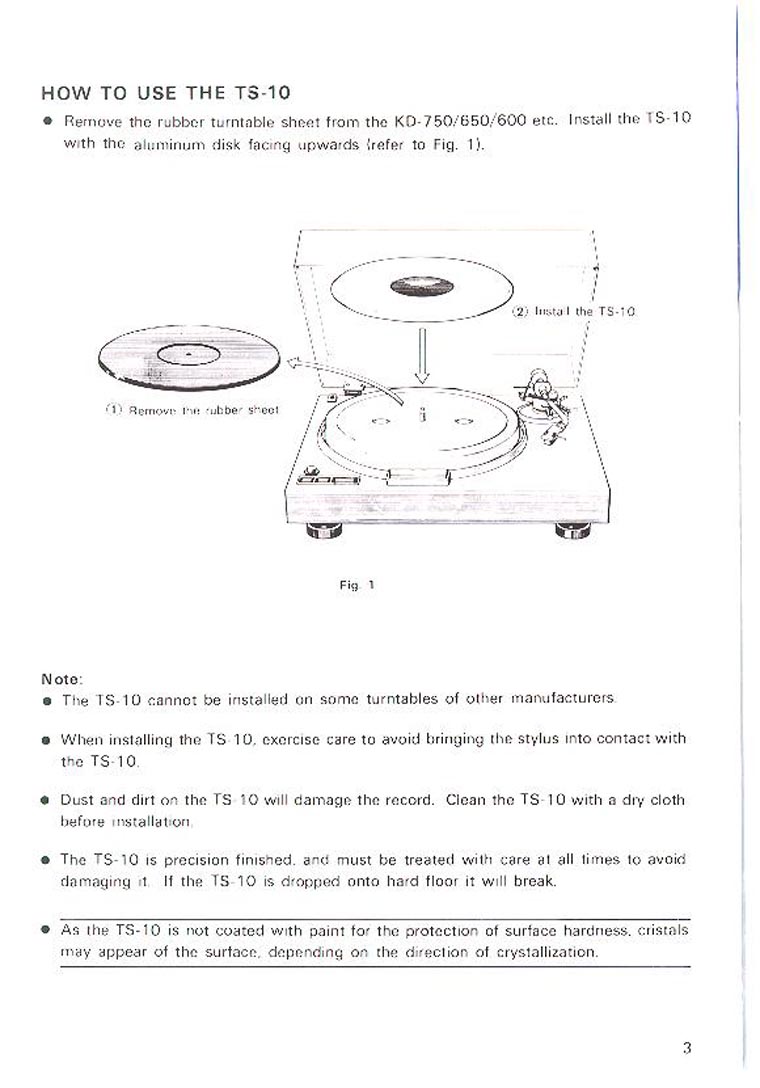
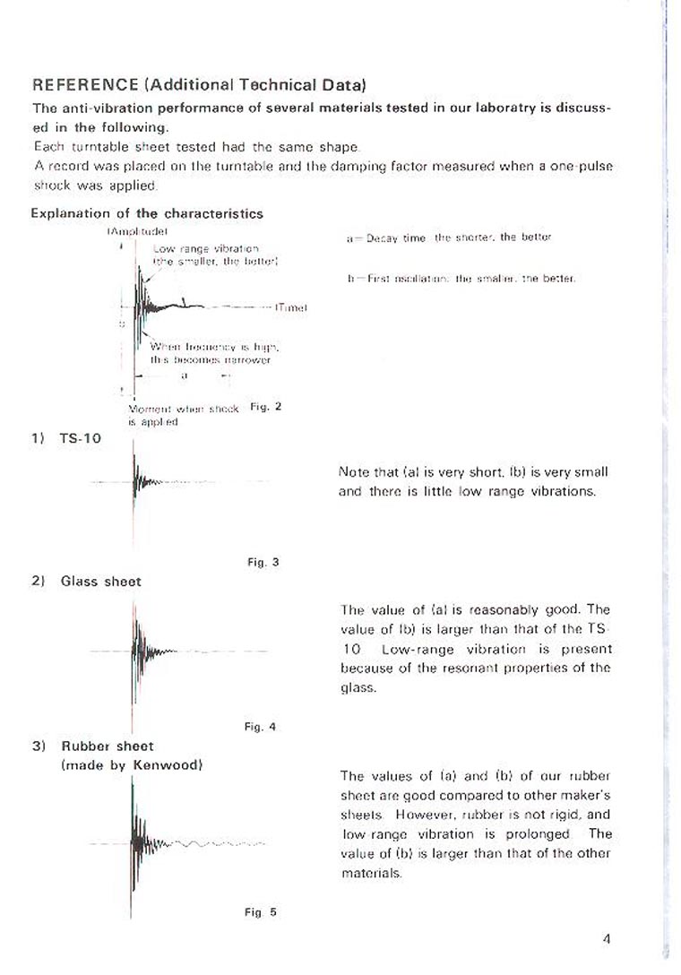
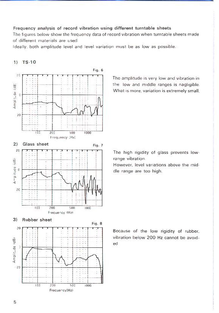
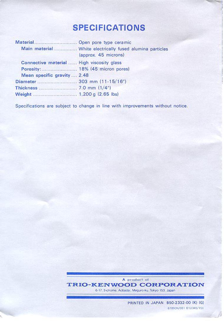
TS-10 Turntable Sheet Guide Book
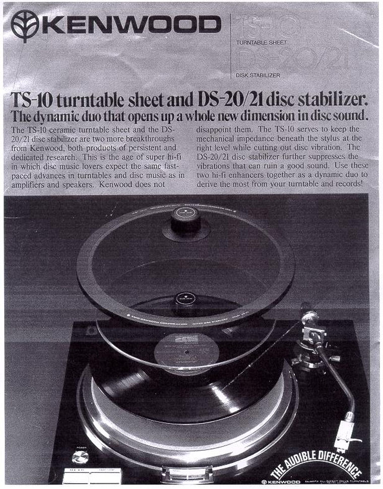
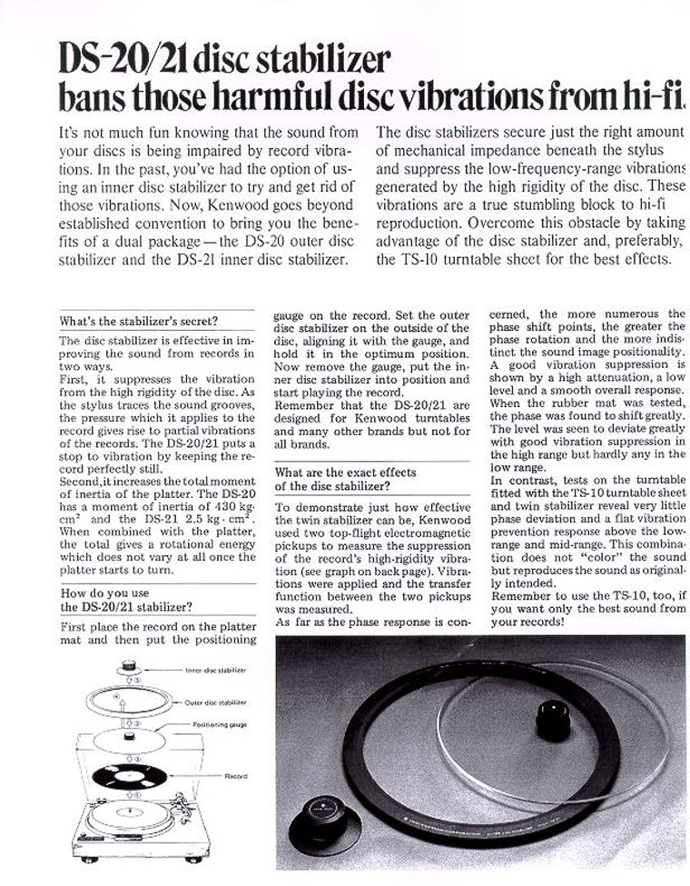
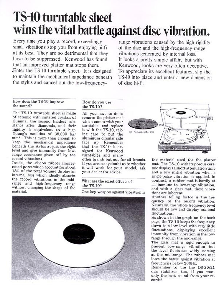
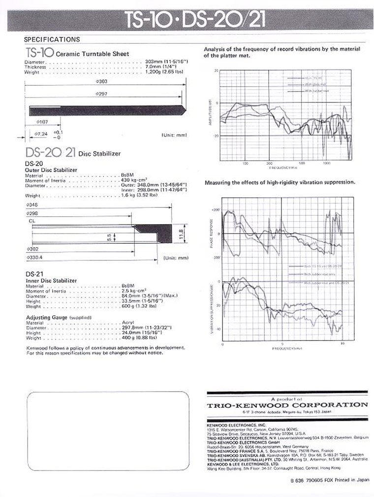
TS-10 Turntable Sheet and DS-20/21 Disc Stabilizer Brochure
English Language Audio Magazine Advertisements
March 1981 "Practical Hi-Fi", advertisement by Subjective Audio
March 1981 "Practical Hi-Fi", advertisement by Bespoke Audio
English Language Review Articles
March 1981 "Practical Hi-Fi", Front Cover
March 1981 "Practical Hi-Fi", article by Dave Berriman, Page 86
March 1981 "Practical Hi-Fi", article by Dave Berriman, Page 87
July 1981 "Practical Hi-Fi", Front Cover
Hi-Fi Choice 1981 Booklet: "Turntables and Tonearms", Front Cover
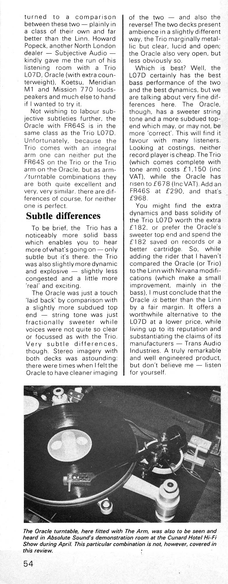
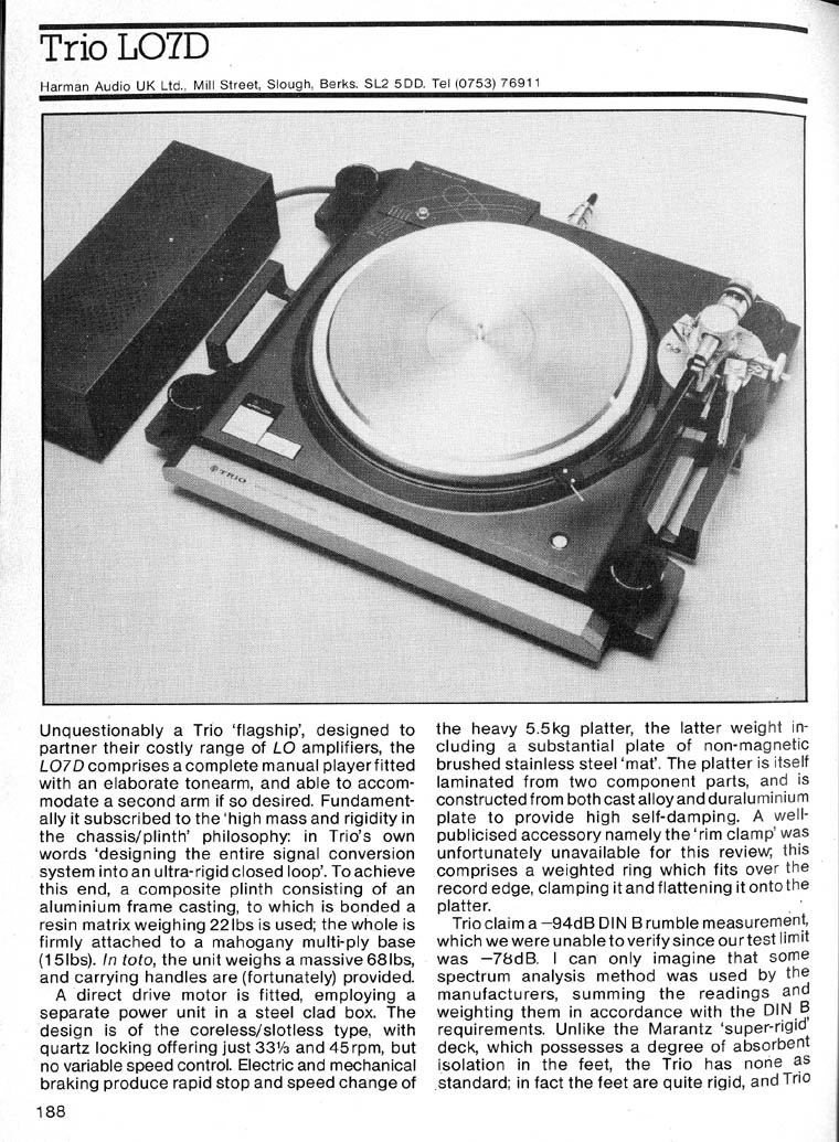
Hi-Fi Choice 1981 Booklet: "Turntables and Tonearms", article by Martin Colloms, Page 188
Hi-Fi Choice 1981 Booklet: "Turntables and Tonearms", article by Martin Colloms, Page 189
Hi-Fi Choice 1981 Booklet: "Turntables and Tonearms", article by Martin Colloms, Page 190
March 1998 "Hi-Fi World", article by Jon Marks
German Language Kenwood Brochures
Brochure entitled "HIFI Extra Dry", L-07D Page 1
Brochure entitled "HIFI Extra Dry", L-07D Page 2
Brochure entitled "Kenwood Hi-Fi Stereo", L-07D Page 1
Brochure entitled "Kenwood Hi-Fi Stereo", L-07D Page 2
German Language Audio Magazine Advertisements
March 1981 "Practical Hi-Fi", advertisement by Kenwood
German Language Review Articles
August 1980 "HIFI exclusiv", Front Cover
August 1980 "HIFI exclusiv", article by Alejandro Wagner, Page 7
August 1980 "HIFI exclusiv", article by Alejandro Wagner, Page 8
August 1980 "HIFI exclusiv", article by Alejandro Wagner, Page 9
August 1980 "HIFI exclusiv", article by Alejandro Wagner, Page 10
August 1980 "HIFI exclusiv", article by Alejandro Wagner, Page 11
August 1980 "HIFI exclusiv", article by Alejandro Wagner, Page 12
March 1981 "Practical Hi-Fi", article by Dave Berriman, Page1
March 1981 "Practical Hi-Fi", article by Dave Berriman, Page 2
March 1981 "Practical Hi-Fi", article by Dave Berriman, Page 3
Italian Language Review Articles
Stereoplay 1981 article by F. Gatta and Roberto Battaglia
English Language translation of Stereoplay 1981 article by Roberto Salafia: r.salafia@tin.it
Cartridge Alignment
L-07D Cartridge Alignment Measurements
Critical measurements for the L-07D tonearm are:
Spindle-to-Pivot distance: 229.5mm
Tonearm Effective Length (Leff): 245.0mm
Spindle Diameter: 0.2825 inches
Calculated Overhang (Baerwald): 16.8mm
Calculated Overhang (Löfgren): 17.2mm
My opinion is that Baerwald alignment (of 16.8mm overhang) sounds better than Löfgren alignment. Baerwald alignment geometrically allows better tracking on the inner grooves. The non-damped ultra-rigid design of the L-07D tonearm mechanism works better at the inner grooves when Baerwald alignment is used.
A Microsoft Excel spreadsheet showing calculation of Baerwald and Löfgren cartridge alignment calculations is posted at:
Kenwood L-07D Baerwald-Löfgren Cartridge Alignment Spreadsheet You can use the tabs at the bottom left of the spreadsheet to toggle between Baerwald and Löfgren spreadsheets.
Author's Recommended Method of Phonographic Cartridge Alignment on the L-07D
For geometry to be correct, overhang and zenith must be perfect at proper VTA. I have used a several alignment tools including a metal Denessen Soundtractor and a Turntable Basics Phono Cartridge Alignment Tool. I have also measured actual overhang beyond the spindle along the overhang line.
Now I only use a custom made for the L-07D Wally Tractor. The Wally Tractor is far superior to any other method and/or device that I have tried in terms of accuracy as it is custom made exactly to the L-07D's tonearm geometry. I have reached the opinion that setting cartridge alignment with any universal cartridge alignment tool will result in imperfect cartridge alignment. For instructions on phono cartridge alignment, the reader is referred to Wally's Complete Turntable Setup Procedure which can be found on Wally Malewicz' web site: Wally's Vinyl Corner. If you order a Wally Tractor, be sure to let Wally know that the spindle diameter is 0.2825 inches.
I use Wally's recommendation to set SRA at 92 degrees. First set VTA so that the headshell is parallel to the record surface at correct VTF and at correct overhang and zenith per alignment protractor. Theoretically SRA should now be at 90 degrees. Now raise the tonearm at the base by 8.59mm to increase SRA 2 degreess to 92 degrees. (1mm increase in SRA = 4.29mm increase in rear arm pivot height). Next, reset overhang and zenith with alignment protractor and reset VTF. I then set azimuth with a non magnetic level on the headshell with the stylus raised off of the LP. You can loosen the headshell collar and then slight play of the headshell allows azimuth adjustment. The slight play is gone after finger tightening the headshell collar.
For setting VTF, forget about balance beam scales. They are not very inaccurate. Use a good digital stylus pressure gauge. Measurement should be taken at record surface level. All alignment parameters will affect VTF, so readjust VTF after completing platter leveling and phono cartridge alignment.
When zenith is properly set, the cartridge will be rotated slightly clockwise from the long axis of the headshell (when the headshell and cartridge are viewed from above). Achieving the necessary degree of cartridge rotation to set zenith correctly is generally not a problem with the L-07D headshell if the cartridge uses full length screws and nuts for attachment. However if the cartridge has fixed threaded screw holes, the captured design of the L-07D headshell finger might not allow sufficient cartridge rotation to set zenith correctly. Therefore, with cartridges that have fixed threaded screw holes and if correct zenith can not be achieved with the original headshell, I recommend the Sumiko HS-12 headshell, which is highly adjustable. I also recommend the Sumiko HS-12 headshell as an excellent alternative to the original L-07D headshell. If you have a Sumiko Flux Buster cartridge demagnitizer, it is very handy to use to position the headshell for final tightening of cartridge attachment hardware, off the tonearm and away from the turntable.
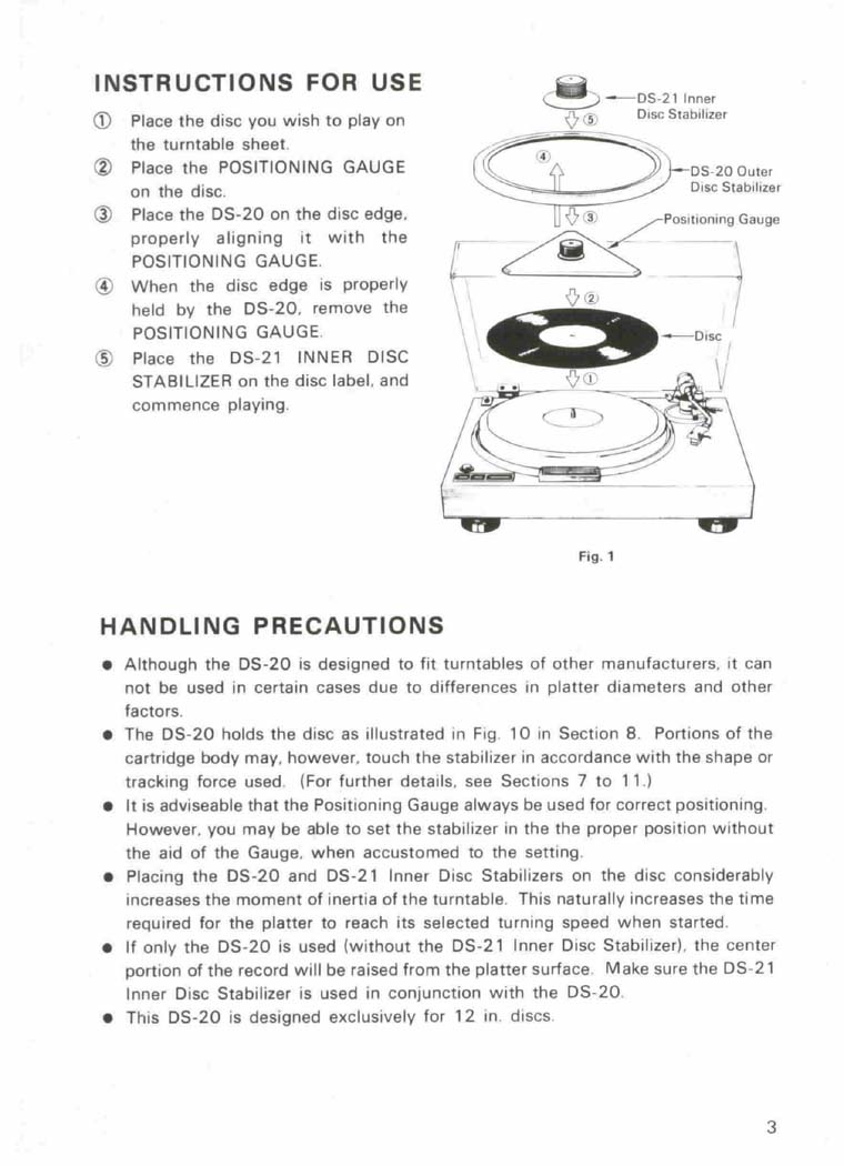
If you are using a DS-20 Outer Disk Stabilizer, pay careful attention to the tonearm cueing mechanism. It is important to prevent the stylus tip from contacting the Outer Disk Stabilizer, particularly when the platter is spinning, to prevent damage to the stylus and/or cartridge cantilever. With VTA optimally adjusted, be sure that the when the tonearm cueing mechanism is raised that the stylus tip is at least a couple of millimeters above the outer portion of the DS-20 (when DS-20 is on a record). If there is not enough clearance (and if there is room to raise the tonearm cueing mechanism cylinder further), adjust the tonearm cueing mechanism height by loosening the Allen grub screw(s) securing the cueing mechanism cylinder to tonearm collar with a 1.5mm metric Allen key. Prior to performing this procedure, the headshell should be removed and the tonearm should be removed from the tonearm base and taken over to a clean work area for this procedure. Do not put any force on the lifter support as you change the cylinder position or you may damage the cueing mechanism internally. Raising the cueing mechanism cylinder in relation to the tonearm collar will provide additional clearance between the stylus and the DS-20 Outer Disk Stabilizer. Re-tighten the Allen grub screw(s) after completing the adjustment. Please note that this procedure can only be done if there was some clearance between the screw securing the lifter support to the cueing piston and the rubber button above it when the tonearm is parked. Do not attempt this procedure if no clearance exists between the screw securing the lifter support to the cueing piston and the rubber button above it when the tonearm is parked.
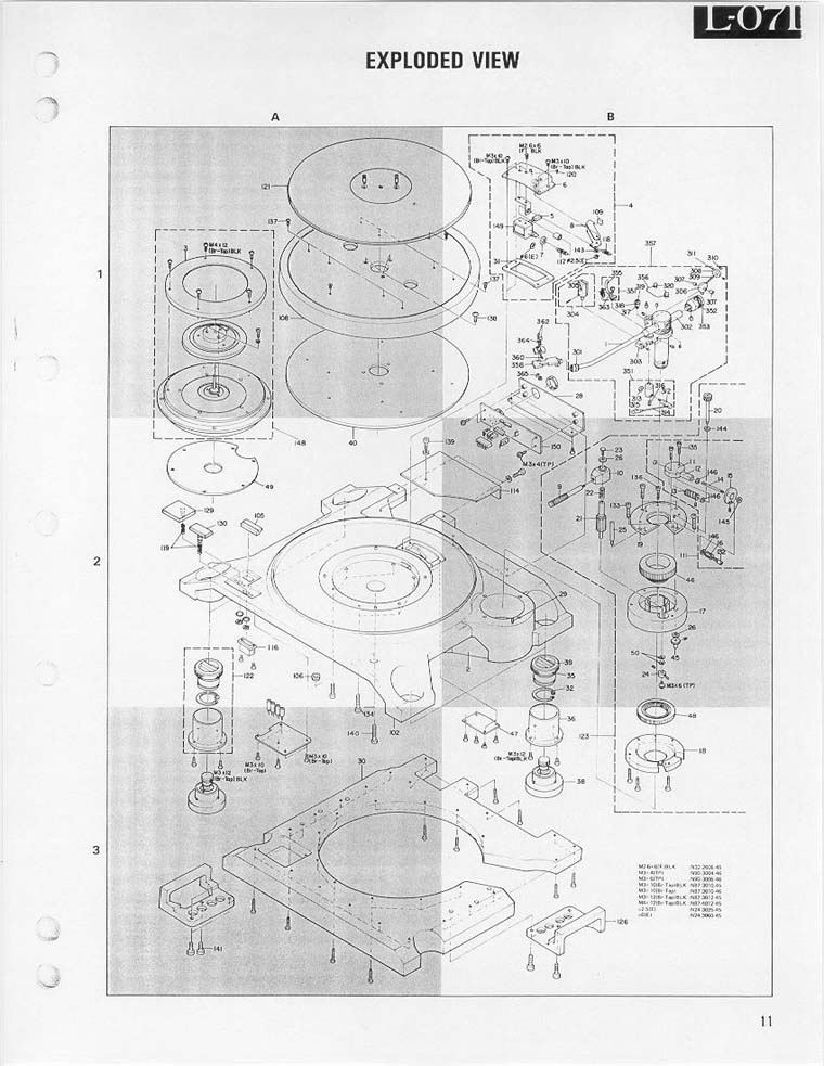
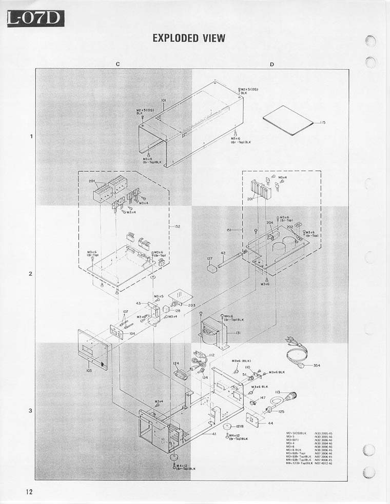
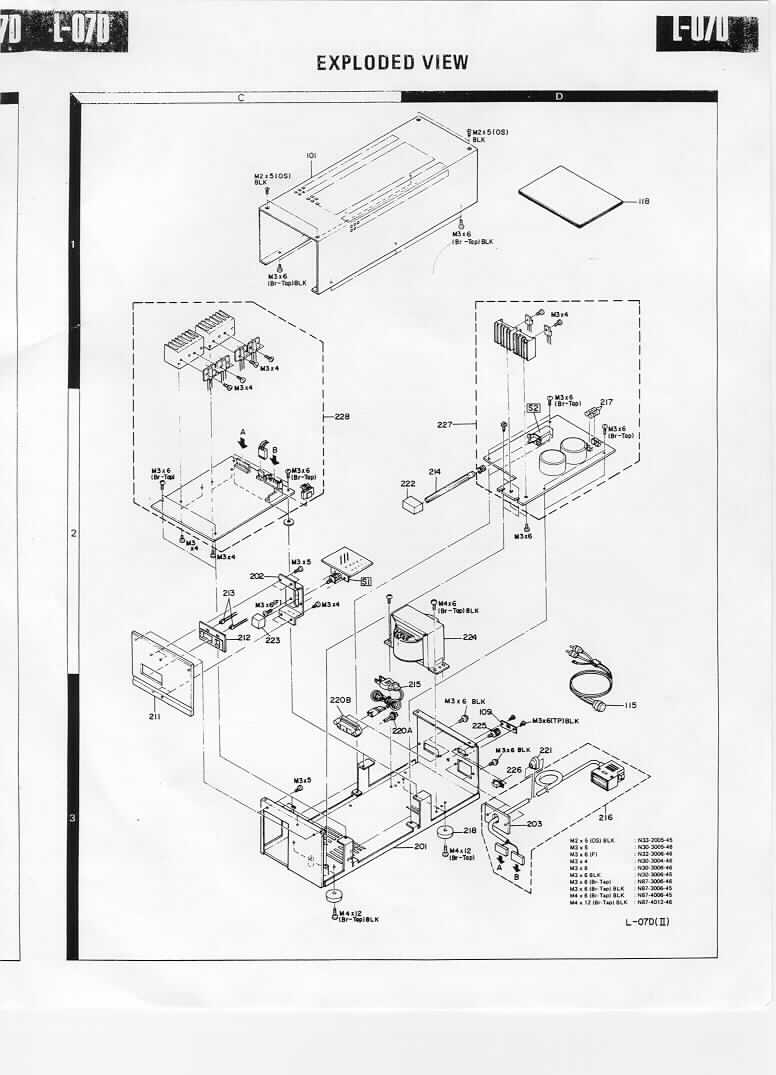
Repair Related Information
I have created some documents which I have developed from the L-07D & L-07D II schematics and service manuals. These documents help me troubleshoot and repair these decks. All values and connections have been verified by me during service and repairs. [Information in brackets is/are replacement part supplier(s) and/or part number(s), see Links page for vendor contact info.] I have reproduced these documents below:
Heat Sink Compound also know as Thermal Grease for transistors on heat sinks: DowSil (formerly Dow Corning) 340
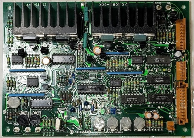
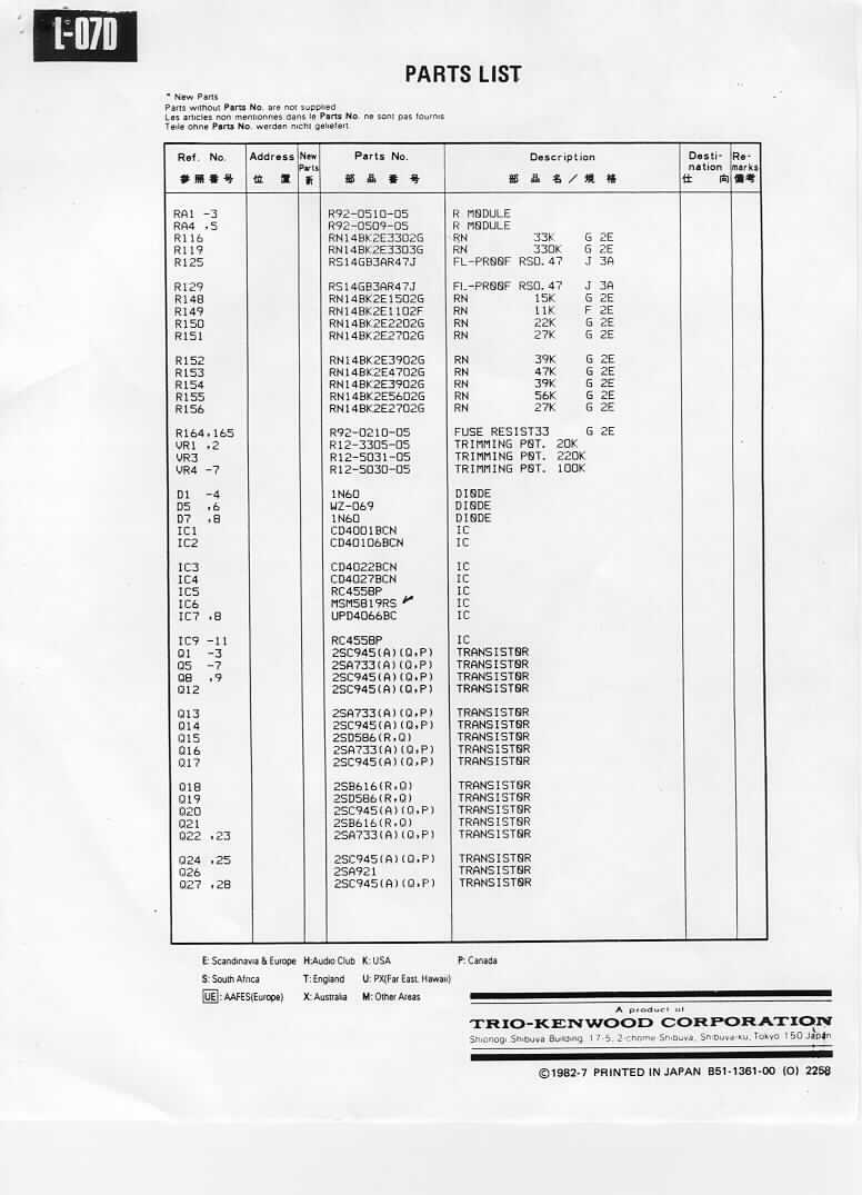
Kenwood L-07D Logic PCB (X29-1180-00) Components and Values
R101 1M
R102 1M
R103 150K
R104 10K
R105 10K
R106 1M
R107 100K
R108 100K
R109 100K
R110 100K
R111 1M
R112 13K
R113 13K
R114 12K
R115 12K
R116 33K (2% Tol)
R117 5.6K
R118 5.6K
R119 330K (2% Tol)
R120 820
R121 820
R122 47K
R123 100K
R125 0.47 1W (On board = 0.82 5W)
R127 47K
R128 100K
R129 0.47 1W (On board = 0.82 5W)
R130 2.2K
R131 2.2K
R132 33K
R133 33K
R134 33K
R135 33K
R136 1.5K
R137 1.5K
R138 5.6K
R139 5.6K
R140 3.3K
R141 3.3K
R142 22K
R143 47K
R144 100K
R145 100K
R146 100K
R148 15K (1% Tol)
R149 11K
R150 22K
R151 27K
R152 39K
R153 47K
R154 39K
R155 56K
R156 27K
R159 1K
R160 1K
R161 220K
R162 220K
R163 2.2K
R164 33 Fused
R165 33 Fused
R168 1M
R182 1M
R183 120K
R184 22K
R185 1M
R186 820
R187 82
R188 82
R189 330K (Incorrectly listed as 680K on page 6 of L-07D II service manual)
R190 330K (Incorrectly listed as 680K on page 6 of L-07D II service manual)
R191 1M
R192 47K (Late model L-07D and all L-07D II only on underside of PCB in circuit from IC10 Pin1 to C115)
R193 47K (Late model L-07D and all L-07D II only on underside of PCB in circuit from IC11 Pin1 to C117)
RA1 10K SIP Resistor Network 12 Leads for 6 Resistors
RA2 10K SIP Resistor Network 12 Leads for 6 Resistors
RA3 10K SIP Resistor Network 12 Leads for 6 Resistors
RA4 100K SIP Resistor Network 10 Leads for 5 Resistors
RA5 100K SIP Resistor Network 10 Leads for 5 Resistors
VR1 22K Trimmer Pot 33 rpm
VR2 22K Trimmer Pot 45 rpm
VR3 220K Trimmer Pot SC1-GAIN
VR4 100K Trimmer Pot BI-2
VR5 100K Trimmer Pot BI-1
VR6 100K Trimmer Pot BO-1
VR7 100K Trimmer Pot BO-2
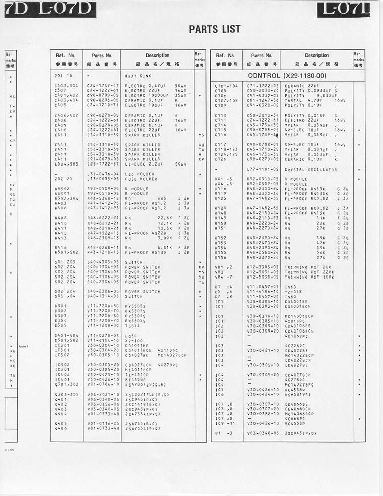
C101 22pf Ceramic [Allied 507-0201], [Radio Shack 272-809], [Mouser 594-CN15A220J]
C102 22pf Ceramic
C103 22pf Ceramic
C104 22pf Ceramic
C105 0.0033uf Mylar [Allied 998-0050]
C106 0.033uf Mylar (Larger than C124 and C125, probably higher voltage) [Allied 862-2206]
C107 4.7uf Tantalum (Tantalum capacitors are polarized with + and – leads) [Allied 852-5651]
C108 4.7uf Tantalum (Tantalum capacitors are polarized with + and – leads)
C109 0.1uf Mylar [Allied 613-0557]
C110 0.01uf Mylar [Allied 862-2200]
C111 22uf 16V Electrolytic [Allied 852-6640]
C114 0.039uf Mylar [Allied 862-2207], [Mouser 667-ECQ-E2393JF]
C115 10uf 16V Non-Polar Electrolytic [NTE NPR10M50]
C116 0.039uf Mylar
C117 10uf 16V Non-Polar Electrolytic
C118 0.001uf Mylar [Allied 998-0044]
C119 0.001uf Mylar
C120 0.001uf Mylar
C121 0.001uf Mylar
C122 0.001uf Mylar
C123 0.001uf Mylar
C124 0.033uf Mylar [Allied 862-2206]
C125 0.033uf Mylar
C126 0.1uf 25V Ceramic [Allied 926-3418] [Vishay Cera-Mite HY850]
C127 2.2uf 50V Long Life Electrolytic [Allied 852-7094]
C128 2.2uf 50V Long Life Electrolytic
IC1 CD4001BCN
IC2 BC40106BCN
IC3 CD4022BCN
IC4 CD4027BCN
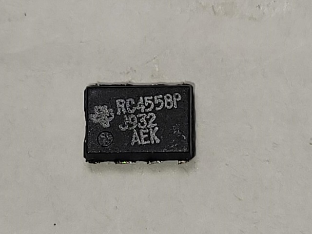
IC5 RC4558P
IC6 MSM5819RS [East Coast Part Number V30-0424-10]
IC7 UPD4066BC
IC8 UPD4066BC
IC9 RC4558P
IC10 RC4558P
IC11 RC4558P
X-tal L77-1101-05 labeled 5.5296 1101-0 TKC-H Schematic Lists X-Tal as 5.5296 MHz
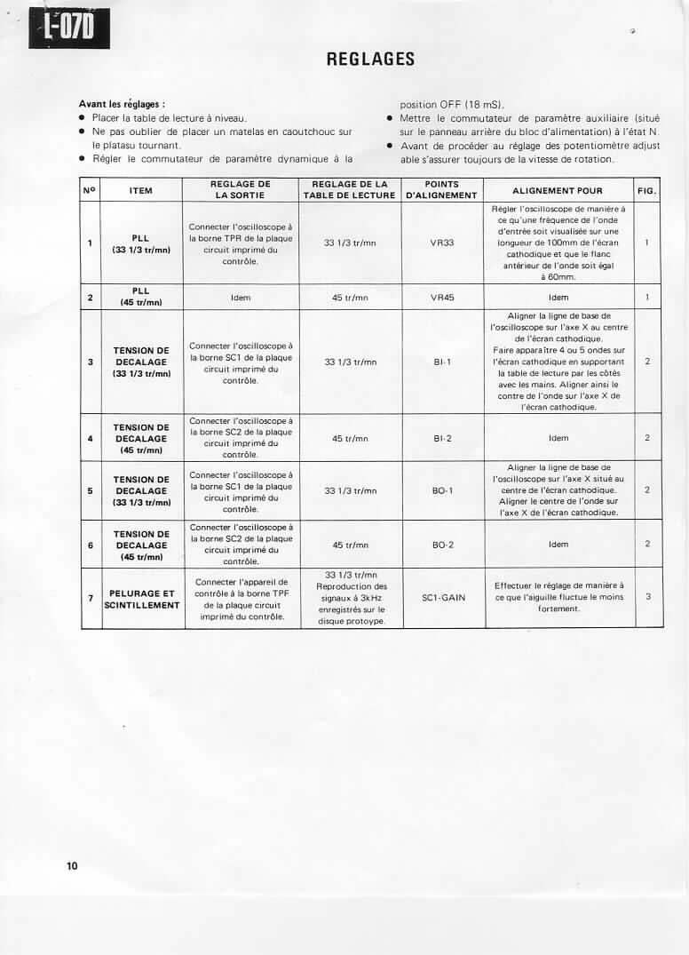
Alignment points: GND, TRP, TPF, SC 1, SC 2
Two dual TO-3 Heat Sinks
Q1 2SC945 [NTE 85]
Q2 2SC945
Q3 2SC945
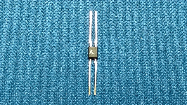
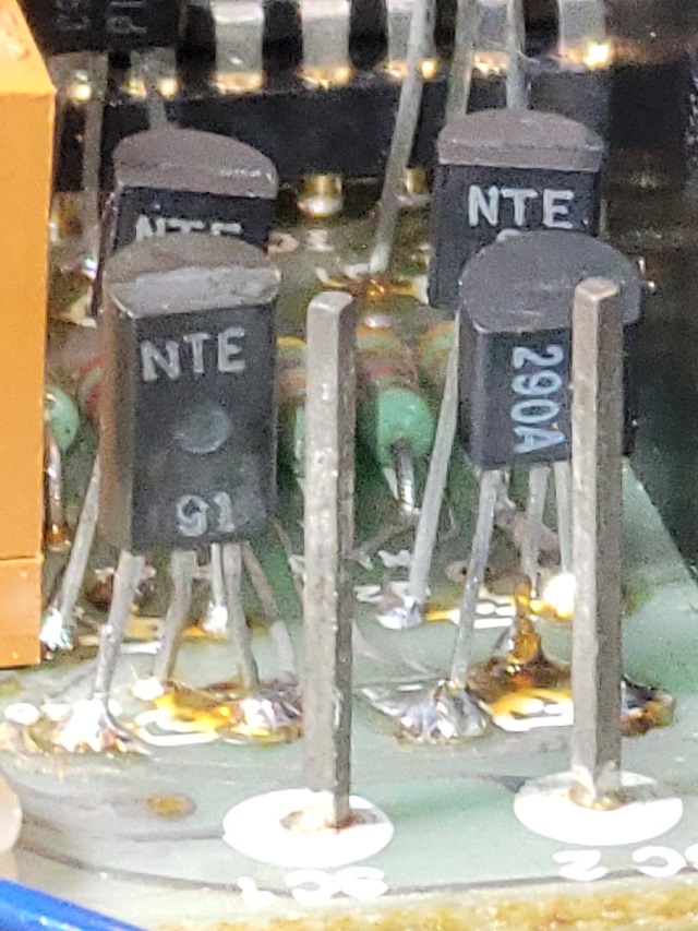
Q5 2SA733 [NTE 290A]
Q6 2SA733
Q7 2SA733
Q8 2SC945
Q9 2SC945
Q12 2SC945
Q13 2SA733
Q14 2SC945
Q15 NECD586 aka 2SD586 (60 Watt Power Transistor 5A/100V/15Mhz Silicon NPN) TO-3 [Obsolete]
Q16 2SA733
Q17 2SC945
Q18 NECB616 aka 2SB616 (60 Watt Power Transistor 5A/100V/15Mhz Silicon PNP) TO-3 [Obsolete]
Q19 NECD586 aka 2SD586
Q20 2SC945
Q21 NECB616 aka 2SB616
Q22 2SA733
Q23 2SA733
Q24 2SC945
Q25 2SC945
Q26 2SA921 Note, some boards substitute 2SA733, if so I replace with [NTE 91]
Q27 2SC945
Q28 2SC945
PH 1 10 pin connecting post. Uses wire wrap posts spaced 0.10 inches apart (Standard IC connector spacing) On L-07D II round leads in white connector spaced 0.10 inch apart.
PH 2 6 pin connecting post. Uses wire wrap posts spaced 0.10 inches apart (Standard IC connector spacing)
PH 3 11 pin connecting post. Uses wire wrap posts spaced 0.10 inches apart (Standard IC connector spacing) On L-07D II round leads in white connector spaced 0.10 inch apart.
PH 4 2 pin connecting post. Uses wire wrap posts spaced 0.10 inches apart (Standard IC connector spacing)
D1 1N60 1N60 replacement is ECG 109, a Germanium general purpose
D2 1N60 diode, max. forward voltage drop is 1 volt at 200ma.
D3 1N60 [NTE 110A] (Germanium)
D4 1N60
D5 WZ-069 [NTE-5071A] (Zener)
D6 WZ-069
D7 1N60
D8 1N60
To convert a Generation I board to an L-07D II board:
1. Interrupt original top trace between (Right/IC8 side of) C115 and Pin 1 of IC 10
2. Solder in 47K resistor on underside of board from (IC8 side of) C115 to Pin 1 of IC 10
3. Interrupt trace on underside between solder point under R120 to solder point under the number “6” of Q6
4. Solder in 47K resistor between solder point under R120 and solder point under the number “6” of Q6
5. Solder in Jumper on underside of board from Pin 10 of IC 8 to (Left/IC8 side of) C117
Low profile IC Sockets:
8 Pin [Mouser 575-113308], [Radio Shack 276-1995]
14 Pin [Mouser 575-113314], [Radio Shack 276-1999]
16 Pin [Mouser 575-113316], [Radio Shack 276-1998]
18 Pin [Mouser 575-113318], [Radio Shack 276-1992]
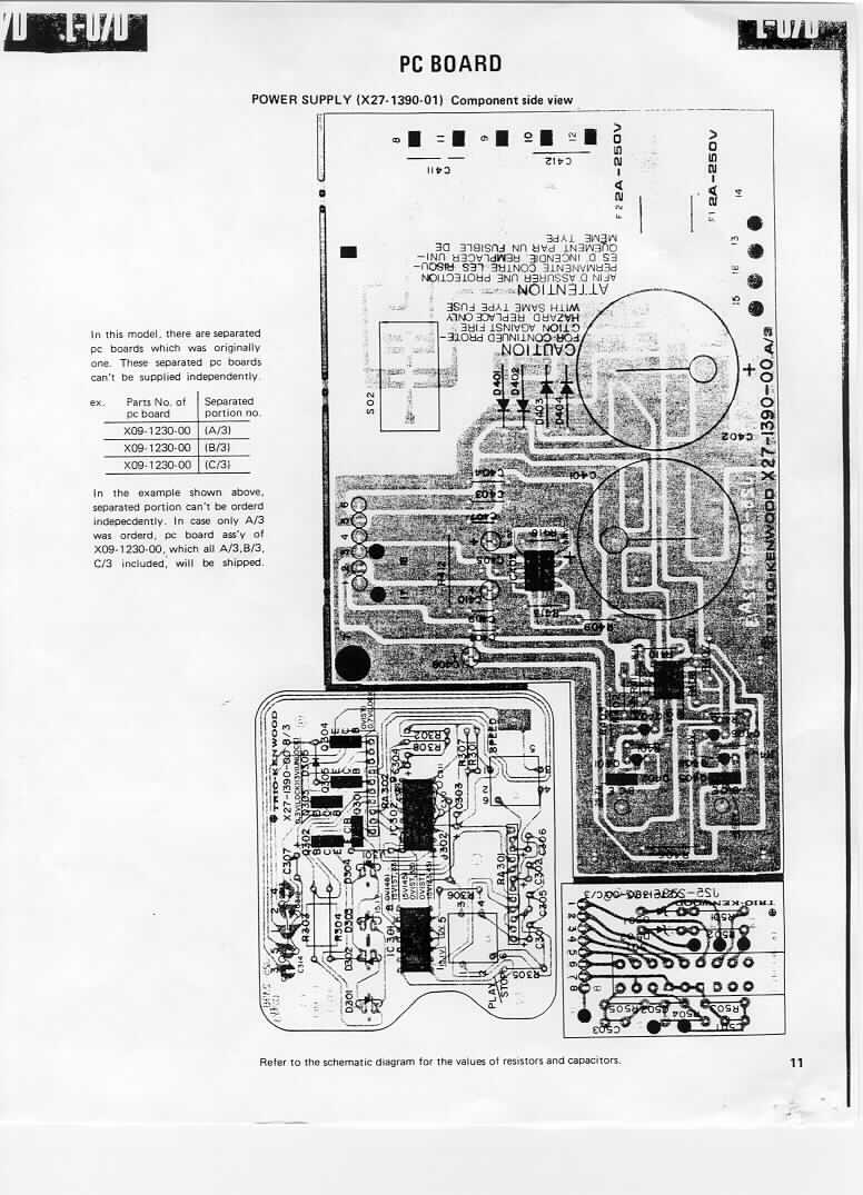
Kenwood L-07D Power Supply PCB (X27-1390-02) Components and Values
R401 8.2K
R402 15K
R403 1.2 1W
R404 8.2K
R405 15K (2% Tol)
R406 1.2 1W
R407 12K
R408 22.6K (1% Tol)
R409 10K
R410 12.1K (1% Tol)
R412 220 2W
R413 3.09K (1% Tol)
R416 6.81K (1% Tol) (Incorrectly listed as 6.18K on page 4 of L-07D II service manual)
C401 10,000uF 35V 85degree ELNA CE69W(P) 40mm Diameter x 30mm Height, 4-Pin PCB Mount
C402 10,000uF 35V 85degree ELNA CE69W(P) 40mm Diameter x 30mm Height, 4-Pin PCB Mount
[BHC ALC10C103EC063 from RS Components part no. 339-8114, available through Allied telephone sales], [Kemet ALC10C103EC063, Mouser Part Number 80-ALC10C103EC063]
C403 0.1uf 50V Ceramic [NTE 89410] [Vishay Cera-Mite HY950]
C404 0.1uf 50V Ceramic
C405 100uf 16V Electrolytic [Allied 852-7079], [Radio Shack 272-1044]
C406 0.1uf 25V Ceramic [Allied 926-3418] [Vishay Cera-Mite HY850]
C407 0.1uf 25V Ceramic
C408 22uf 16V Electrolytic [Allied 852-6640]
C409 0.1uf 25V Ceramic
C410 22uf 16V Electrolytic
C411 0.01uf Polypropylene Across-the-line RFI Suppression Line Filter X-Capacitor [Vishay F1772 Class X2]
Q401 2SC945
Q402 2SC1419 [NTE 152, TIP 31A (Allied 935-0995)]
Q403 2SC945
Q404 2SA733
Q405 2SB514 [NTE 153, TIP 32A (Allied 935-1000)]
Q406 2SA733
D401 Hitachi U05B Glass Bead Rectifier Diode 100V [Radio Shack 276-1143, 3A, 200PIV for 120VAC USA only use]
D402 Hitachi U05B Glass Bead Rectifier Diode 100V [Radio Shack 276-1144, 3A, 400PIV for 120VAC - 220VAC international use], [Mouser 863-MR854G]
D403 Hitachi U05B Glass Bead Rectifier Diode 100V
D404 Hitachi U05B Glass Bead Rectifier Diode 100V
IC401 RC4558P
IC402 TL431CP
2A 250v Fast Blow Fuses (2)
Spring loaded single pole on-off push switch
Wrapping Posts #’s 13, 14, 15, 16 and 17
Six Lead wire set soldered to PCB #’s 1, 2, 3, 4, 5 and 6
Two single TO-220 Heat Sinks
Flat Post 12 No Connection
Flat Post 10 Big red wire
Flat Post 9 Small red wire
Flat Post 11 Big white wire
Flat Post 8 Small white wire
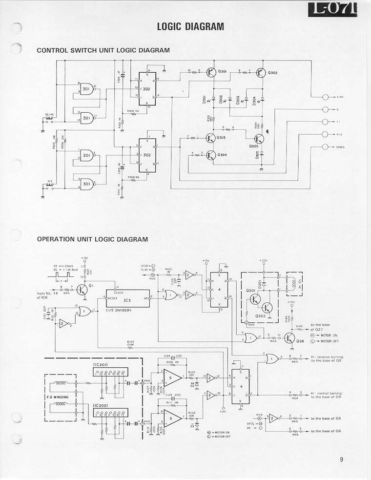
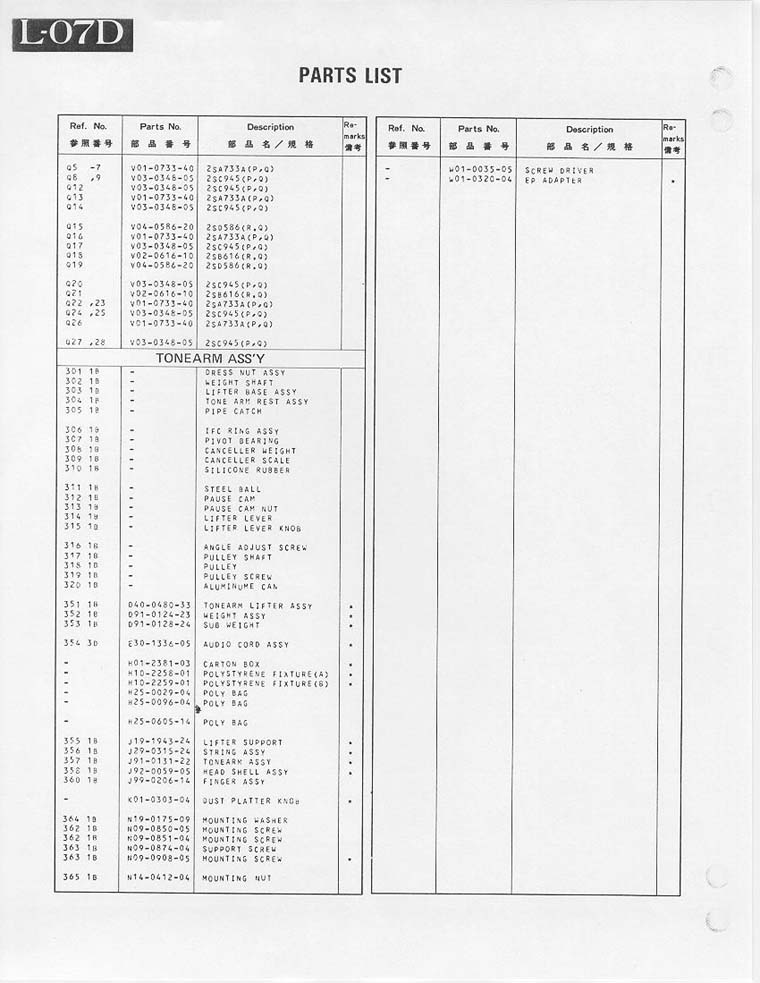
Kenwood L-07D Switching PCB (X27-1390-00) Components and Values
R301 1M
R302 1M
RA302 10K SIP Resistor Network 10 Leads for 5 Resistors
R303 680 (1/2 watt)
R304 680 (1/2 watt)
R305 10K
R306 10K
R307 10K
R308 10K
RA301 10K SIP Resistor Network 12 Leads for 6 Resistors
RA302 100K SIP Resistor Network 10 Leads for 5 Resistors
C301 0.01uf Mylar
C302 0.01uf Mylar
C303 0.47uF 50V Electrolytic [NTE NEV.47M50AA]
C304 0.47uF 50V Electrolytic
C305 0.01uf Mylar
C306 0.01uf Mylar
C307 22uf 16V Electrolytic [Mouser 647-UVZ1J220MDH]
IC301 CD4011BE
IC302 CD4027BE
Q301 C2021S:Q
Q302 C2021S:Q
Q303 C2021S:Q
Q304 C2021S:Q
Q305 C2021S:Q
D301 GREEN L.E.D. FOR 45 RPM [Calrad Electronics Part Number 92-120-GN]
D302 RED L.E.D. FOR 33 RPM [Calrad Electronics Part Number 92-120-RD]
D303 GREEN L.E.D. FOR 45 RPM [Calrad Electronics Part Number 92-120-GN]
D304 RED L.E.D. FOR 33 RPM [Calrad Electronics Part Number 92-120-RD]
D305
PLAY/STOP SWITCH
SPEED SWITCH
Kenwood L-07D Connector PCB (X25-1550-00) Components and Values
R1 100K
R2 1M (Service manual incorrectly list this resistor as 680K)
R3 100K
R4 680K (Service manual incorrectly list this resistor as 1M)
R5 100K
R6 1K
R7 1K
R8 1K
R9 1K
Beware of factory defect PCB that is missing R4!!! Unit will intermittently not quartz lock at 33 RPM!
C1 10uf 16V Electrolytic [Allied 998-1369]
C2 10uf 16V Electrolytic
C3 10uf 16V Electrolytic
C4 10uf 16V Electrolytic
C5 0.1uf 25V Ceramic [Mouser 80-C052C104K5R molded or Allied 926-3418 ceramic] [Vishay Cera-Mite HY850]
C6 0.1uf 25V Ceramic
IC1 TA7136P [Obsolete, can substitute with TA7136AP which is also obsolete]
IC2 TA7136P
Q201 2SC945
Q202 2SD882 [Obsolete]
D1 W06B [NTE-116] (Low Power switching 600V general purpose Silicon rectifier diode)
L1 180 uH Inductor [TOKO 822MY-181K avail. from Digi-Key TK4482-ND]
L2 180 uH Inductor [TOKO 822MY-181K avail. from Digi-Key TK4482-ND]
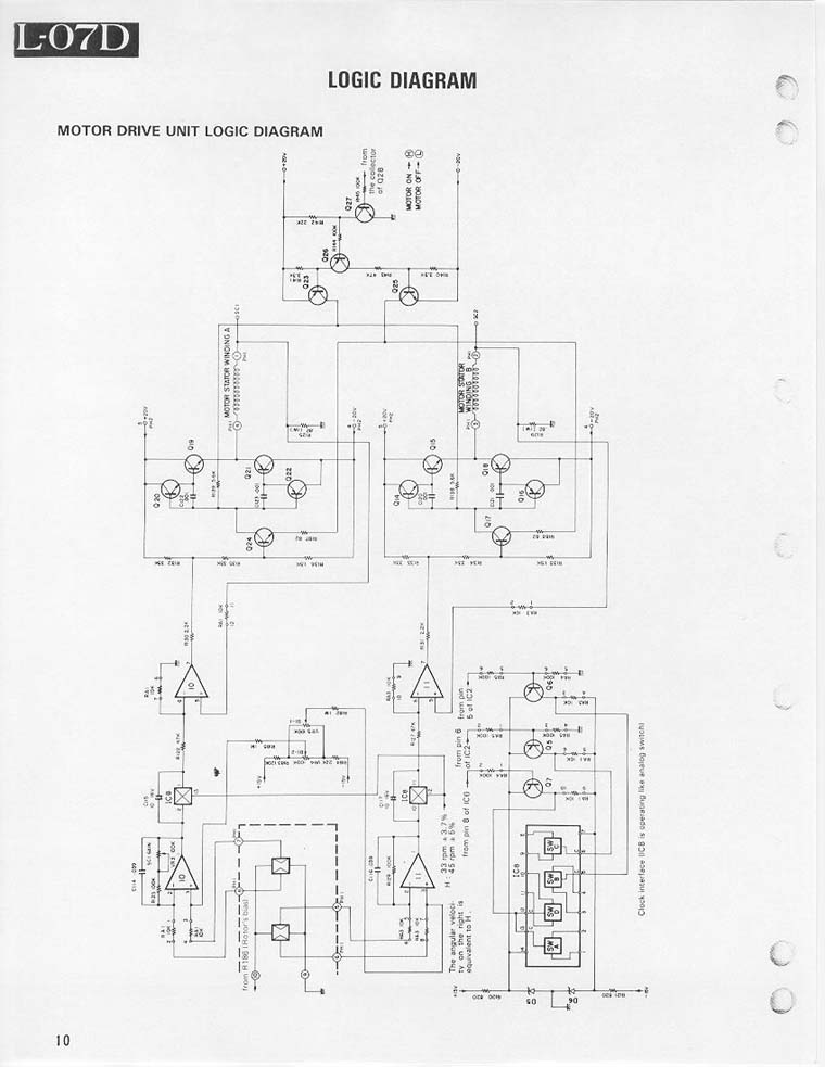
Kenwood L-07D Motor - Wiring and Measurements
PH-1:
1 Grey – Power to deep coil
2 Black – Common ground to both coils
3 Red – Power to superficial coil
4 Blue – Power to deep coil
5 Green – To pin 2 of rear Hall element
6 Orange – To pin 4 of rear Hall element
7 Yellow – To pin 2 of front Hall element
8 Brown – To pin 4 of front Hall element
9 Violet – To pins 3 of both Hall elements
10 Grey – To pins 1 of both Hall elements
Resistances of coils:
Superficial = 14.9 ohms
Deep = 14.8 ohms
Typical resistances of Hall elements:
Pins 1-2 250 - 350
Pins1-3 166 (330 in series)
Pins 1-4 250 - 320
Pins 2-3 250 - 500
Pins 2-4 330 - 440
Pins3-4 250 – 320
PH-2:
Red & Black wires to outer coil of bottom PCB
Blue & White wires to inner coil of bottom PCB
Pins 1-2 = 2.1 ohms
Pins 3-4 = 2.4 ohms
Hall elements (also known as Hall sensors): [Asahi Kasei Microdevices (AKM) HW-300A - Rank A Specification] PDF info sheet: http://www.datasheet-pdf.com/PDF/HW300A-Datasheet-Hall-499550
Now obsolete Asahi Kasei Microdevices (AKM) HW-300A Hall element sensors were made in multiple Ranks (or specifications, or types) of millivolt outputs ranging from Ranks A-H. The higher the letter rank, the greater the millivolt output. Ranks in the datasheet noted above are for Ranks A-F. The correct subtype for the L-07D motor is Rank A, which may also be referred to as Specification A or Type A. The Hall elements may have the letter of the Rank visible on the Hall element itself. The best match to the original will have the letter A visible on the Hall element, signifying that it is Rank A.
Note: Hall elements used in the motor are SMD's (Surface Mount Devices). A low-voltage soldering station with a very fine-tip iron, and magnification, are recommended for Hall element replacement work. Trim Hall element leads to length of original before soldering. This task requires advanced soldering skills. A dot on the Hall element signifies lead 1. Make sure to orient the Hall element correctly when replacing!
Obsolete Rank A Asahi Kasei Microdevices (AKM) HW-300A Hall element sensor shown above.
If you decide to use Rank or Specification B Hall elements (which have a higher output voltage than Rank or Specification A Hall elements), I would replace the Hall elements in pairs so that both Hall elements will be producing the same voltage. I have heard from another technician that after doing so replacing both Hall elements with Rank or Specification B Hall elements, that when the unit was sitting stationary at idle with platter not rotating that there was slightly over 2v across the Hall devices. Looking at the HW-300A spec sheet, that's slightly above the rating curve and after replacing the 820Ω R186 driving resistor with a 1K resistor, there was about 1.7v across the Hall sensors at idle, which is acceptable.
Operation:
Hall element 1 controls motor coil A
Hall element 2 controls motor coil B
During start and stop, both coils are energized together.
Once quartz lock is attained, the coils only get energized alternatively; i.e. coil A on, B off and vice-versa.
This ensures a smoother motor operation as now the rotational energization is passed on from one star tip to the next in succession.
Kenwood L-07D Logic PCB IC Continuity List.
This table lists the next point in the continuity chain for each IC pin. Use this list to check for open circuits before/after IC replacement. Also use to check any IC’s previously replaced. For resistors and capacitors, a continuity tester will read continuity on only one side of the resistor or capacitor. If a continuity tester reads open circuit on both sides of the resistor or capacitor, that would indicate a fault (open circuit). Always check adjacent pins on IC’s for shorts due to soldering. I prefer to use sockets when replacing IC’s. I prefer low profile IC sockets. On a good board, the solder will flow through from bottom to top and catch the top trace. Use flux on both top and bottom traces. Solder wick works best for de-soldering.
This list was made based upon schematics in the service manual and large schematic, and verified with continuity tester testing on a properly working PCB.
IC1 Pin 1 IC4 Pin 2
IC1 Pin 2 (Q- of J-K Flip-Flop A), IC4 Pin 14
IC1 Pin 3 Pin 8 of RA4 (H: Brake Signal)
IC1 Pin 4 Pin 2 of PH3, via pin 9 of RA5
IC1 Pin 5 IC1 Pin 8
IC1 Pin 6 IC4 Pin 15
IC1 Pin 7 C101
IC1 Pin 8 IC1 Pin 5, R102,
IC1 Pin 9 IC3 Pin 4
IC1 Pin 10 IC2 Pin 3,
IC1 Pin 11 IC3 Pin 15
IC1 Pin 12 IC2 Pin 2
IC1 Pin 13 C101, R101
IC1 Pin 14 Pin 1 of PH2
IC2 Pin 1 TPF, IC4 Pin 6
IC2 Pin 2 IC1 Pin 12
IC2 Pin 3 IC1 Pin 10
IC2 Pin 4 IC4 Pin 12
IC2 Pin 5 IC7 Pin 12 & 13, Pin 6 of RA5
IC2 Pin 6 Pin 2 of RA5
IC2 Pin 7 C101, Pin 2 of PH2
IC2 Pin 8 IC4 Pin 13
IC2 Pin 9 R102, C102
IC2 Pin 10 IC4 Pin 6, TPF
IC2 Pin 11 D1
IC2 Pin 12 IC4 Pin 5
IC2 Pin 13 D2
IC2 Pin 14 IC3 Pin 16, Pin 1 of PH2
IC3 Pin 1 (IC3 is a 1/5 Octal Counter)
IC3 Pin 2
IC3 Pin 3
IC3 Pin 4 IC1 Pin 9
IC3 Pin 5
IC3 Pin 6
IC3 Pin 7
IC3 Pin 8 IC3 Pin 13
IC3 Pin 9
IC3 Pin 10
IC3 Pin 11
IC3 Pin 12
IC3 Pin 13 IC3 Pin 8, IC4 Pin 4, Pin 2 of PH2
IC3 Pin 14(Clock) Collector of Q1
IC3 Pin 15(Reset) R103, IC1 Pin 11
IC3 Pin 16 IC2 Pin 14, Pin 1 of PH2
IC4 Pin 1 (Q of J-K Flip-Flop B) (IC4 is a J-K Flip-Flop)
IC4 Pin 2 (Q- of J-K Flip-Flop A) IC1 Pin 1
IC4 Pin 3 R103
IC4 Pin 4 (R of J-K Flip-Flop B) IC3 Pin 13, Ground
IC4 Pin 5 (K of J-K Flip-Flop IC2 Pin 12
IC4 Pin 6 (J of J-K Flip Flop B) TPF, IC2 Pin10
IC4 Pin 7 (S of J-K Flip-Flop B) Ground,
IC4 Pin 8 IC4 Pin 4 & Pin 7
IC4 Pin 9 (S of J-K Flip-Flop A) Emitter of Q1, IC4 Pin 8
IC4 Pin 10 (J of J-K Flip-Flop A) IC4 Pin 11, +15.2V
IC4 Pin 11 (K of J-K Flip-Flop A) IC4 Pin 10, +15.2V
IC4 Pin 12 (R of Flip-Flop A) IC2 Pin 4
IC4 Pin 13 (C of J-K Flip-Flop A) IC2 Pin 8
IC4 Pin 14 (Q- of J-K Flip-Flop A) IC1 Pin 2
IC4 Pin 15 (Q of J-K Flip-Flop A) IC1 Pin 6
IC4 Pin 16 IC4 Pins 10 & 11, +15.2V
IC5 Pin 1 R105
IC5 Pin 2 R106
IC5 Pin 3 R108
IC5 Pin 4 Pin 3 of PH3, -15.2V
IC5 Pin 5 R109
IC5 Pin 6 R110
IC5 Pin 7 R111, R104
IC5 Pin 8 Pin 1 of PH2, +15.2V
IC6 Pin 1 (CP In) IC6 Pin 15
IC6 Pin 2 (V/S Out) R148
IC6 Pin 3 (V/S In) IC8 Pin 4
IC6 Pin 4 (FG In) R113 and R115
IC6 Pin 5 (F/V RC) R116, Base of Q2, C106
IC6 Pin 6 (f/V HC) C105
IC6 Pin 7 (F/V Out) R149
IC6 Pin 8 (LD Out) Pin 2 of RA4 and then Pin 11 of PH3
IC6 Pin 9 (Ground) C109, C110 Ground
IC6 Pin 10 (P/D Out) R151
IC6 Pin 11 (P/D HC) C110
IC6 Pin 12 (P/D RC) TPR
IC6 Pin 13 (1/20 – 1/27 Select) R112, R114
IC6 Pin 14 (ST Out) Pin 8 of RA 5
IC6 Pin 15 (CP Out) IC6 Pin 1
IC6 Pin 16 (X-Tal) 5.5296MHz X-Tal (C103 side)
IC6 Pin 17 (X-Tal) 5.5296MHz X-Tal (C104 side)
IC6 Pin 18 (VDD) D4, Pin 6 of PH2, +8V
IC7 Pin 1 IC7 Pin3
IC7 Pin 2 R150
IC7 Pin 3 IC7 Pin1
IC7 Pin 4 R149
IC7 Pin 5 IC7 Pin 6, IC2 Pin 6
IC7 Pin 6 IC7 Pin 5, IC2 Pin 6
IC7 Pin 7 R118
IC7 Pin 8 R151
IC7 Pin 9 IC7 Pin 11
IC7 Pin 10 R152
IC7 Pin 11 IC7 Pin 9
IC7 Pin 12 IC7 Pin 13, IC2 Pin5
IC7 Pin 13 IC7 Pin 12, IC2 Pin5
IC7 Pin 14 Pin 9 of RA2
(IC8 is a Clock Interface/Quad Switch/Both-Way Analog Switch)
IC8 Pin 1 C115
IC8 Pin 2 C115 (other side of C115), IC10 Pin 1 (on Logic cards without R192 &R193)
IC8 Pin 3 VR2 (45rpm) Switch A = Pins 1,2,13
IC8 Pin 4 IC8 Pin 9, IC6 Pin 3 Switch B = Pins 3,4,5
IC8 Pin 5 Collector of Q6
IC8 Pin 6 Collector of Q5 Switch C = Pins 6,8,19
IC8 Pin 7 Pin 5 of RA-1, D6
IC8 Pin 8 VR1 (33rpm)
IC8 Pin 9 IC8 Pin 4, IC6 Pin 3
IC8 Pin 10 C117 Switch D = Pins 10,11,12
IC8 Pin 11 C117 (other side of C117)
IC8 Pin 12 Pin 13 of IC8, Collector of Q7
IC8 Pin 13 Pin 12 of IC8, Collector of Q7
IC8 Pin 14 R120, Emitter of Q7, D5
IC9 Pin 1 R159, R160
IC9 Pin 2 Emitter of Q9
IC9 Pin 3 R148, Pin 8 of RA2
IC9 Pin 4 R121, Collector of Q13
IC9 Pin 5 Pin 1 of RA2
IC9 Pin 6 D7, D8
IC9 Pin 7 Pin 3 of RA2
IC9 Pin 8 R162, Pin 9 of RA2, Collector of Q12
IC10 Pin 1 SC-1 Gain (VR-3), C115 on , IC8 Pin 2 on on Logic cards without R192 &R193
IC10 Pin 2 R123
IC10 Pin 3 R185
IC10 Pin 4 R121, R161, IC11 Pin 4, -15.2V
IC10 Pin 5 R168
IC10 Pin 6 Pin 7 of RA-1, R122
IC10 Pin 7 R130
IC10 Pin 8 R120, +15.2V
IC11 Pin 1 R128, C117 on Logic cards without R192 &R193
IC11 Pin 2 Other side of R128
IC11 Pin 3 R182
IC11 Pin 4 IC10 Pin 4, -15.2V
IC11 Pin 5 R191
IC11 Pin 6 R127
IC11 Pin 7 R131
IC11 Pin 8 R120, +15.2V
Connector Continuity Data
The following continuity information is useful for tracing problems in the umbilical between the Control Unit and the Turntable connector. This information is also useful if a bad connection or adjacent connector short occurs inside the main connector, and a wire needs to be directed to a different pin:
Inside the X25-1550-00 Connector PCB receptacle, the 24 pins are defined in four rows labeled A through C and six columns labeled 1 through 6.
Inside the X25-1550-00 Connector PCB receptacle, the following pins are in continuity:
B2 to B3 to B4
A6 to D1
D2 to D3
On the logic PCB, the following pins are in continuity:
PH1 pin1 to PH1 pin 2 to PH1 pin 9
The following table indicates the continuity points for the umbilical wiring:
A1 to pin 6 of PH3
A2 to pin11 of PH3
A3 to pin 9 of PH3
A4 to pin 1 of PH3
A5 to pin 2 of PH3
A6 to pin 4 of PH1
B1 to pin 5 of PH3
B2 to pin 4 of PH3
B3 no connection
B4 no connection
B5 to pin 6 of PH1
B6 to pin 5 of PH1
C1 to pin 3 of PH3
C2 to Pin 7 of PH3
C3 to pin 10 of PH3
C4 no connection
C5 no connection
C6 to pin 7 of PH1
D1 to pin 1 of PH1
D2 to pin 2 of PH1
D3 to pin 3 of PH1
D4 to pin 10 of PH1
D5 to pin 9 of PH1
D6 to pin 8 of PH1
Pin 1 of PH1 to D1
Pin 2 of PH1 to D2
Pin 3 of PH1 to D3
Pin 4 of PH1 to A6
Pin 5 of PH1 to B6
Pin 6 of PH1 to B5
Pin 7 of PH1 to C6
Pin 8 of PH1 to D6
Pin 9 of PH1 to D5
Pin 10 of PH1 to D4
Pin 1 of PH3 to A4
Pin 2 of PH3 to A5
Pin 3 of PH3 to C1
Pin 4 of PH3 to B2
Pin 5 of PH3 to B1
Pin 6 of PH3 to A1
Pin 7 of PH3 to C2
Pin 8 of PH3 no connection
Pin 9 of PH3 to A3
Pin 10 of PH3 to C3
Pin 11 of PH3 to A2
Kenwood L-07D Faults Associated with a Failed Component
Unit starts without pushing operation button, speed indicator momentarily hits GREEN but continues to speed up and stays RED, pushing operation button does not stop unit – Bad IC2.
Solenoid clicks when powered up at 33 rpm before operation button is pushed. If operation button is pushed (at 33 rpm) unit will quartz lock. If operation button is pushed again, unit will stop and solenoid will resume clicking once platter stops. If switched to 45 rpm, unit will turn backwards and will not stop when operation button is pressed again. - Bad IC 2.
Unit starts but speed indicator never turns GREEN, platter over-speeds. Operation button slows platter with much less force than normal - Bad IC 2.
Unit starts and quartz locks normally at 33 and 45 rpm. When operation button is pushed mechanical brake chatters (Solenoid clicking) and works ineffectively. Mechanical brake chatter stops when platter stops. - Bad IC 2.
Unit powers on normally with platter motionless before operation button is pushed. Engagement of solenoid brake occurs almost silently at power-up, without the usual audible click. Unit will quartz lock when operation button is pushed. When operation button is pushed again, platter will slow to a stop and then continue to rock back and forth, brake solenoid doesn't deploy. Pushing operation button again, unit will play and quartz lock, but same phenomenon when the operation button is pushed again; platter will slow to a stop and then continue to rock back and forth, brake solenoid doesn't deploy - Bad IC 3.
Speed indicator flashes RED-GREEN, runs at correct speed but won’t quartz lock – Bad IC 6.
When the Operation button is pushed, the platter gradually increases speed but over-speeds. Speed indicator doesn’t turn GREEN. Pushing the Operation button again results in platter stopping a few minutes later (Mechanical brake correctly activates with click sound and platter stops) - Bad IC 7.
Motor buzzing when platter is stopped due to electronic brake remaining on - Bad Q23.
Platter gently rocks back and forth at startup, but will not spin. If started with a push, it will spin but will not quartz lock - bad C102.
Speed indicator flashes RED-GREEN and depending on the position of the rotor platter will start alone or just rock backward and forward - bad C119 allowing DC on the B winding.
Unit goes to hyper-speed, speed indicator never flashes GREEN. Brake works properly – Bad L1 and L2 inductors on X25-1550-00 Connector PCB.
Unit occasionally won't quartz lock at 33 rpm - Check for factory defect in X25-1550-00 Connector PCB. I have found one made without R4.
Unit starts and plays normally. Only problem is clattering sound from motor during electronic braking. Braking function is otherwise normal. - Bad capacitors on X25-1550-00 Connector PCB. Replace 0.1uf Ceramic capacitors (2), replace and upgrade 10uf electrolytic capacitors (4).
Unit starts and plays normally. Only problem is mechanical brake engages as soon as Operation button is pushed to stop platter rotation. Braking function is otherwise normal including electronic braking. (Mechanical brake is not supposed to engage until electronic brake has slowed platter to 1/5 of operating speed,) – Bad IC 2.
Platter over-speeds momentarily for about 1/2 turn (kick) before it returns to lock mode. This happens every 10-15 sec.– Bad front Hall element.
Poor start-up torque – Bad rear Hall element.
Rubbing sound in motor - Possibility #1: Magnetic pad has de-laminated from underside of rotor. Do not run unit until repairs are made. Possibility #2: Thrust bushing wear has allowed magnetic pad on underside of rotor to rub FG Coil PCB screws. Repair by disassembling thrust bushing mechanism. Flip bushing over to expose unworn side and reassemble with a new O-ring and lubricate bearing. Do not run unit until repairs are made. Possibility #3: Stator coil wires rubbing against the rotor. Repair by gently pulling all wires exiting the motor thereby removing slack in all wires. Do not run unit until repairs are made. Possibility #4: Rotor is contacting some portion of stator. Repair by inserting a brass washer shim between each stator screw bushing and the motor housing to increase clearance between rotor and stator. Ensure that each motor cover screw will pass though a brass washer shim to hold the shims in place after reassembly. Do not run unit until repairs are made.
When the unit is powered up, both speed indicators (33 & 45 RPM) are on at same time (RED) instead of one. When the speed button is pressed, 33 RPM speed indicator turns off, 45 RPM speed indicator remains on (RED), press the speed button once again and 33 & 45 RPM are again on at same time (RED). (45 RPM speed indicator never turns off.) Unit will only play at 33RPM, either with speed indicator reading 45 RPM quartz lock (GREEN) but actual speed is 33 RPM, or if speed button is pushed will again quartz lock at 33 RPM with both speed indicator LEDs staying on at the same time (33 & 45 RPM speed indicators both (GREEN). (45 RPM speed indicator never turns off.) – Bad IC 301 and 302 on switching PCB.
PLL waveform not stable, noise in AC signal driving the motor - Bad 0.001 uf capacitor.
Fixed voltage output from IC 10 or from IC 11 - bad corresponding Hall element.
Failure to phase lock - solved by replacing C105, 106, 109, 110.
Intermittent quartz lock failure - stray strand of wire from jumper on undersurface of logic card intermittently making contact with adjacent component lead solder point.
From Nick Gorham: Internally they were untouched and in good condition, but on powering up the control unit the platter started to rotate at 33RPM, running perfectly, but switches had zero effect and none of the LED's lit. After trying all the obvious like checking the connecting cable. I eventually removed the switch PCB and running it on a bench supply is wasn't working. Replaced IC301 and 302 but made no difference. Finally traced the fault to be broken earth/0v continuity as the trace went to and from R301. I can only assume the board had flexed and broken the trace. added wire links to mimic the traces to and from R301 and then it worked as expected on the bench. Replaced it into the turntable and it all works fine. Checked setup, it was almost perfect so left well alone. Power rails were +- 27v so again the transformer was never a good match for UK supply which while officially 230v, it almost always over 240v (mine is 246 normally).
Unit quartz locks but the motor buzzes intermittently when stopped. Disconnecting the mechanical brake makes no difference, confirming that the buzzing is from the motor. This occurs intermittently for around a second at a time. It is most notable just after turning the Control Unit on. Thereafter the occurrences happen anywhere from minutes to hours apart. Occasionally, the platter will turn backwards a small amount when the buzzing occurs, but not usually. Changing the position of the Dynamic Parameter Switch makes no difference. The buzzing occurrences are seen as positive voltage spikes at test point (TP) SC2 and as negative voltage spikes at TP TPR. No voltage spikes are seen during occurrences at TP SC1, however. Below are some DSO images of the occurrences sampling from TP SC2:
![]()
![]()
The fault was a bad signal transistor, one or more of Q1, Q26, Q27 and Q28, all of which I changed out together. The bad transistor(s) tested good in circuit but had the failure under power. At some point, Kenwood replaced the 2SA733 amplifier transistor at Q26 with a 2SA921 high-gain amplifier transistor. I wonder if they saw similar or different issues with Q26 that caused them to make this change. When I see a unit for service that has a 2SA733 at Q26, I replace it with a 2SA921 equivalent (NTE 91):
Unit turns at set speed but playback sound has speed instability. This can occur with or without a rubbing sound from the motor. On the oscilloscope, there is instability of the PLL waveform sampled at TPR (video links below). There is also similar instability of the square wave sampled at TPF.
With the turntable operating at 33 RPM, the waveform instability occurs 33 times per minute. 
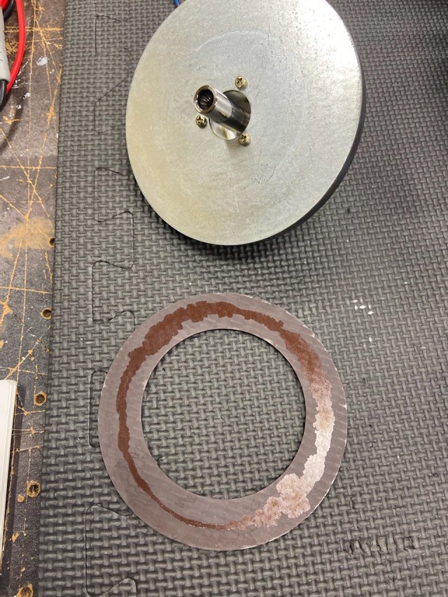
The cause of this fault is a delaminated and eccentrically-shifted magnetic pad on the underside of the rotor. The magnetic pad remains adherent to the rotor plate due to magnetism. The glue bond has failed and the magnet has shifted to an eccentric location on the rotor plate as shown in the photo below:
The photo below shows that the glue that bonds the round magnetic pad to the rotor plate has failed.
General Tips from Experience
It is easiest to test the logic board transistors after removing all the capacitors at the time of capacitor replacement.
When servicing the power supply board in the Control Unit, the board will need to be turned between top side up and bottom side up a number of times to replace caps, rectifiers, etc. This will put repeated strain on the wiring from the transformer to the power supply board and the wiring from the mains in to the power supply board. To prevent this wire strain from occurring and causing wire breakage, turn the transformer with the power supply board each time. Otherwise the repeated strain will cause wires to break at their solder points.
When recapping the power supply board, it is easiest to use a spring clip heat sink on the small capacitors when soldering in replacements if the front 10,000uf filter capacitor is off the board, i.e. removed and before the new replacement filter capacitor is soldered in.
Due to some thin traces, some logic PCB traces most prone to trace damage during capacitor removal: C114, C116, C115, C117 in particular. Extra caution and gentle technique for desoldering and removal are recommended for these logic PCB caps. Cap splitting, shown and discussed below, can help minimize the chance of trace damage during capacitor removal.
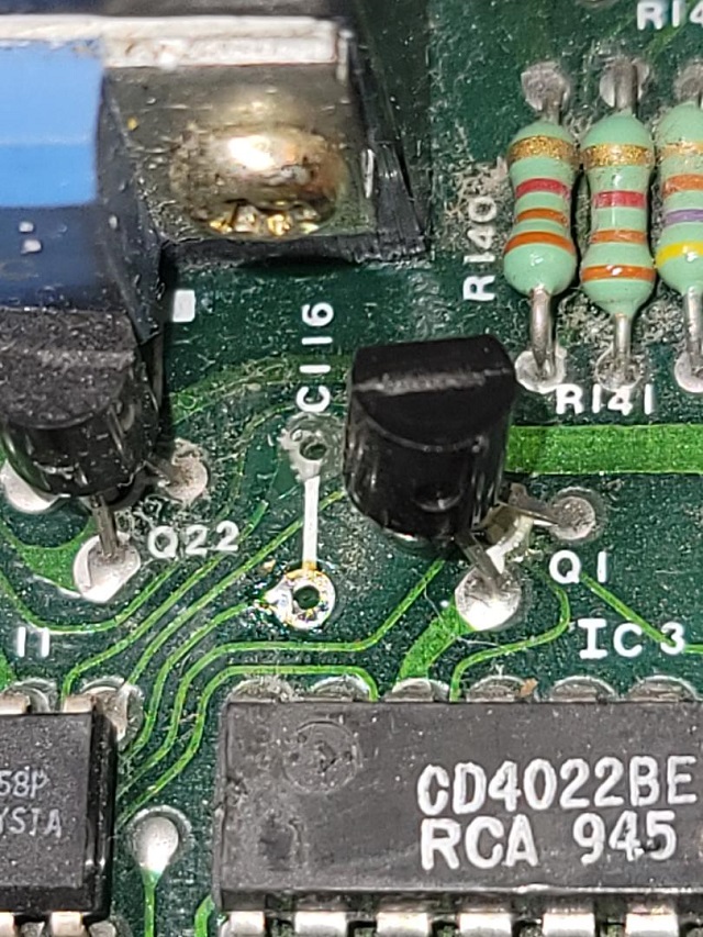
Trace damage that occurred during removal of C116 without splitting the cap first is shown above. Trace repair can be done by exposing the copper on the remaining end of the trace for 3-4 millimeters and soldering wire from the trace to the replacement capacitor pin, or with a jumper wire on the bottom of the PCB.
The small paper capacitors (C118, C119, C120, C121, C122, C123) are easier to remove, and removal is less likely to cause PCB trace damage, if they are split vertically in two before removal. Then the individual pins can be pulled axially during removal without having to cant the cap sideways during removal.
In the photo above C119 has been vertically split with a 6 inch cutter prior to removal.
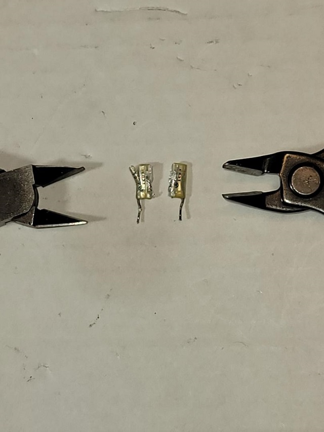
In the photo above, a removed split 0.001uf paper cap is shown with small cutters used to split the cap.
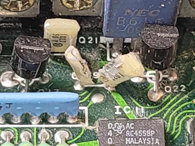
The larger paper caps on the logic board (C114, C116, C124 and C125) are easier to remove, and less likely to cause PCB trace damage, if they are split vertically in two before removal. These caps require a somewhat larger cutter than the 0.001uf paper caps. The double-action 8 inch cutter shown in one of the photos below works well for this purpose.
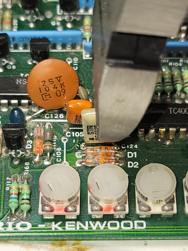
Splitting larger paper cap C124 shown above with 8-inch double action cutter.
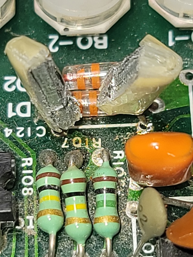
One of the larger paper caps on the logic PCB (C124) is shown vertically split in the photo above prior to removal.
The 8-inch double action cutter shown above works well for splitting the larger paper caps on the logic PCB prior to removal.
For integrated circuit removal, PCB traces are much less likely to be damaged if the IC pins are cut from the IC body, and then the IC body removed, prior to IC pin desoldering and pin removal from the PCB.
Shown in the photo above, the IC pins were cut off from the body of the IC right where the pins exit the body. Then the IC body was lifted away from the PCB. After doing so the IC pins on the PCB are fully accessible for individual desoldering from both sides of the PCB.
Logic PCB shown above after removal of all paper and film caps with no trace damage.
Disclaimer
1. Content
The author reserves the right not to be responsible for the topicality, correctness, completeness or quality of the information provided. Liability claims regarding damage caused by the use of any information provided, including any kind of information which is incomplete or incorrect, will therefore be rejected. All offers are not-binding and without obligation. Parts of the pages or the complete publication including all offers and information might be extended, changed or partly or completely deleted by the author without separate announcement. This site provides no warranty, expressed or implied, as to the accuracy, reliability or completeness of furnished data. This disclaimer applies to all portions, pages, images and text applicable to this entire website.
2. Referrals and links
The author is not responsible for any contents linked or referred to from his pages - unless he has full knowledge of illegal contents and would be able to prevent the visitors of his site from viewing those pages. If any damage occurs by the use of information presented there, only the author of the respective pages might be liable, not the one who has linked to these pages. Furthermore the author is not liable for any postings or messages published by users of discussion boards, guest-books or mailing lists provided on his page.
3. Copyright
The copyright for any material created by the author is reserved. Any duplication or use of objects such as diagrams, sounds or texts in other electronic or printed publications is not permitted without the author's agreement.
4. Privacy policy
If the opportunity for the input of personal or business data (e-mail addresses, name, addresses) is given, the input of these data takes place voluntarily. The use and payment of all offered services are permitted - if and so far technically possible and reasonable - without specification of any personal data or under specification of anonymous data or an alias. The use of published postal addresses, telephone or fax numbers and e-mail addresses for marketing purposes is prohibited, offenders sending unwanted spam messages will be punished.
5. Legal validity of this disclaimer
This disclaimer is to be regarded as part of the internet publication which you were referred from. If sections or individual terms of this statement are not legal or correct, the content or validity of the other parts remain uninfluenced by this fact.
All trademarks and rights belong to the OEM and are reproduced here for information purposes only. Copyright © 2003-2022. All rights reserved.